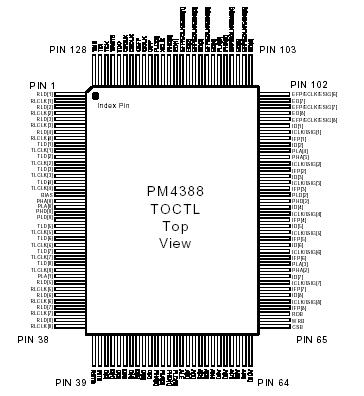
Features: ` Integrates eight T1 framers in a single device for terminating duplex DS-1 signals.
` Supports SF and ESF format DS-1 signals.
` Supports transfer of PCM data to/from 1.544 MHz system-side devices. Also supports a fractional T1 system interface with independent ingress/egress NxDS0 rates. Supports a 2.048 MHz system-side interface without external clock gapping.
` Provides jitter attenuation in the receive and transmit directions.
` Provides per-DS0 line loopback and per link diagnostic and line loopbacks.
` Provides an integral pattern generator/detector that may be programmed to generate and detect common pseudo-random or repetitive sequences. The programmed sequence may be inserted/detected in the entire DS-1 frame, or on an NxDS0 basis, in both the ingress and egress directions. May be configured to transmit or detect in only the 7 most significant bits of selected channels, in order to support fractional T1 loopback codes in an N x 56kbps fractional T1 setup. Each framer possesses its own independent pattern generator/detector, and each detector counts pattern errors using a 32-bit saturating error counter.
` Provides robbed bit signaling extraction and insertion on a per-DS0 basis.
` Provides programmable idle code substitution, data and sign inversion, and digital milliwatt code insertion on a per-DS0 basis.
` Software compatible with the PM4341A T1XC Single T1 Transceiver and the PM4344 TQUAD Quad T1 Framer.
` Seamless interface to the PM8313 D3MX single chip M13 multiplex and to the PM4314 QDSX Quad Line Interface.
` Provides an 8-bit microprocessor bus interface for configuration, control, and status monitoring.
` Low power 3.3V CMOS technology with 5V tolerant inputs.
` Supports standard 5 signal P1149.1 JTAG boundary scan.
` Available in a 14 mm by 20 mm 128 pin Plastic Quad Flat Pack (PQFP) or an 11mm by 11mm 128 pin Chip Array Ball Grid Array (CABGA) package.
Each one of eight receiver sections:
` Accepts gapped data streams to support higher rate demultiplexing.
` Provides Red, Yellow, and AIS alarms integration.
` Provides programmable in-band loopback code detection.
` Indicates signaling state change, and 2 superframes of signaling debounce on a per-DS0 basis.
` Provides an HDLC interface with 128 bytes of buffering for terminating the facility data link.
` Provides performance monitoring counters sufficiently large as to allow performance monitor counter polling at a minimum rate of once per second. Optionally, updates the performance monitoring counters and interrupts the microprocessor once per second, timed to the receive line.
` Provides an optional elastic store which may be used to time the ingress streams to a common clock and frame alignment, or to facilitate per-DS0 loopbacks.
Each one of eight transmitter sections:
` May be timed to its associated receive clock (loop timing) or may derive its timing from a common egress clock or a common transmit clock; the transmit line clock may be synthesized from an N*8kHz reference.
` Provides minimum ones density through Bell (bit 7), GTE or "jammed bit 8" zero code suppression on a per-DS0 basis.Provides a 128 byte buffer to allow insertion of the facility data link using the host interface.
` Supports transmission of the alarm indication signal (AIS) or the Yellow alarm signal in both SF and ESF formats.
` Provides a digital phase locked loop for generation of a low jitter transmit clock.
` Provides a FIFO buffer for jitter attenuation and rate conversion in the transmitter.
Application· High density Internet T1 interfaces for multiplexers, switches, routers and digital modems.
· Frame Relay switches and access devices (FRADS)
· SONET/SDH Add Drop MultiplexersPinout Specifications
| Case Temperature under Bias |
-55°C to +125°C |
| Storage Temperature |
-65°C to +150°C |
| Voltage on VDD with Respect to GND |
-0.3V to 4.6V |
| Voltage on BIAS with respect to GND |
VDD - 0.3V to 5.5V |
| Voltage on Any Pin |
-0.3V to BIAS + 0.3V |
| Static Discharge Voltage |
±1000V |
| Latch-Up Current |
±100mA |
| DC Input Current |
±20mA |
| Lead Temperature |
+230°C |
| Junction Temperature |
+150°C |
DescriptionThe PM4388 Octal T1 Framer (TOCTL) is a feature-rich device for use primarily in systems carrying data (frame relay, Point to Point Protocol, or other protocols) over DS-1 facilities. Each of the framers and transmitters is independently software configurable, allowing feature selection without changes to external wiring.
On the receive side, each of eight independent framers can be configured to frame to either of the common DS-1 signal formats: (SF, ESF) or to be bypassed (unframed mode). The TOCTL detects and indicates the presence of Yellow and AIS patterns and also integrates Yellow, Red, and AIS alarms.
Performance monitoring with accumulation of CRC-6 errors, framing bit errors, out-of-frame events, and changes of frame alignment is provided. The TOCTL PM4388 also detects the presence of in-band loopback codes, ESF bit oriented codes, and detects and terminates HDLC messages on the ESF data link. The HDLC messages are terminated in a 128 byte FIFO. An elastic store that optionally supports slip buffering and adaptation to backplane timing is provided, as is a signaling extractor that supports signaling debounce, signaling freezing and interrupt on signaling state change on a per-DS0 basis. The TOCTL PM4388 also supports idle code substitution and detection, digital milliwatt code insertion, data extraction, trunk conditioning, data sign and magnitude inversion, and pattern generation or detection on a per-DS0 basis.
On the transmit side, the TOCTL PM4388 generates framing for SF or ESF DS-1 formats, or framing can be optionally disabled. The TOCTL PM4388 supports signaling insertion, idle code substitution, data insertion, line loopback, data inversion, zero-code suppression, and pattern generation or detection on a per-DS0 basis.
The TOCTL PM4388 can generate a low jitter transmit clock from a variety of clock references, and also provides jitter attenuation in the receive path.
The TOCTL provides a parallel microprocessor interface for controlling the operation of the TOCTL device. Serial PCM interfaces allow 1.544 Mbit/s ingress/egress system interfaces to be directly supported. Tolerance of gapped clocks allows other backplane rates to be supported with a minimum of external logic.
It should be noted that the TOCTL device operates on unipolar data only: B8ZS substitution and line code violation monitoring, if required, must be processed by the T1 LIU.

 PM4388 Data Sheet


