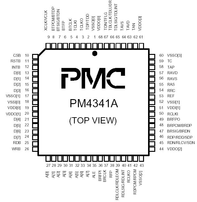
Features: · Integrates a full-featured T1 framer and line interface in a single device with analog circuitry for receiving and transmitting DSX-1 compatible signals and digital circuitry for terminating the duplex DS-1 signal.
· Provides an 8-bit microprocessor bus interface for configuration, control, and status monitoring.
· Low power CMOS technology
· Available in either a 68 pin PLCC package, or a high density (14 by 14mm) 80 pin PQFP package.
The receiver section:
· Provides analog circuitry for receiving a DSX-1 signal up to 655 feet from the cross-connect. Direct digital inputs are also provided to allow for by-passing the analog front-end.
· Recovers clock and data using a digital phase locked loop for high jitter tolerance. A direct clock input is provided to allow clock recovery to be bypassed.
· Accepts dual rail or single rail digital PCM inputs.
· Supports B8ZS or AMI line code.
· Accepts gapped data streams to support higher rate demultiplexing.
· Frames to SF, ESF, T1DM (DDS), and SLC®96 format DS1 signals.
· Provides loss of signal detection, and red, yellow, and AIS alarm detection. Red, yellow, and AIS alarms are integrated as per industry specifications.
· Detects violations of the ANSI T1.403 12.5% pulse density rule over a moving 192 bit window.
· Provides programmable in-band loopback code detection.
· Supports line and path performance monitoring according to AT&T and ANSI specifications. Accumulators are provided for counting:
· ESF CRC-6 errors to 333 per second;
· Framing bit errors to 31 per second;
· Line code violations to 4095 per second; and
· Loss of frame or change of frame alignment events to 7 per second.
· Provides ESF bit-oriented code detection, and an HDLC/LAPD interface for terminating the ESF data link.
· Supports polled, interrupt-driven, or DMA servicing of the HDLC interface.
· Extracts the data link in ESF, T1DM (DDS) or SLC®96 modes. Extracts the Dchannel for Primary Rate interfaces.
· Provides a two-frame elastic store buffer for jitter and wander attenuation that performs controlled slips and indicates slip occurrence and direction.
· Provides robbed bit signalling extraction, with optional data inversion, programmable idle code substitution, digital milliwatt code substitution, bit fixing, and 2 superframes of signalling debounce on a per-channel basis.
· Provides trunk conditioning which forces programmable trouble code substitution and signalling conditioning on all channels or on selected channels.
· Optionally provides dual rail digital PCM output signals to allow BPV transparency. Also supports unframed mode.
· Supports transfer of received PCM and signalling data to 1.544 Mbit/s backplane buses or to 2.048 Mbit/s backplane buses.
The transmitter section:
· Supports transfer of transmitted PCM and signalling data from 1.544 Mbit/s or 2.048 Mbit/s backplane buses.
· Formats data to SF, ESF, T1DM (DDS), and SLC®96 format DS1 signals.
· Optionally accepts dual rail digital PCM inputs to allow BPV transparency. Also supports unframed mode and framing bit, CRC, or data link by-pass.
· Provides signalling insertion, programmable idle code substitution, digital milliwatt code substitution, and data inversion on a per channel basis.
· Provides trunk conditioning which forces programmable trouble code substitution and signalling conditioning on all channels or on selected channels.
· Provides minimum ones density through Bell (bit 7), GTE or DDS zero code suppression on a per channel basis.
· Detects violations of the ANSI T1.403 12.5% pulse density rule over a moving 192 bit window or optionally stuffs ones to maintain minimum ones density.
· Allows insertion of framed or unframed in-band loopback code sequences.
· Allows insertion of a data link in ESF, T1DM (DDS) or SLC®96 modes. Allows insertion of the D- channel for Primary Rate interfaces.
· Supports transmission of the alarm indication signal (AIS) or the yellow alarm signal in all formats.
· Provides ESF bit-oriented code generation and an HDLC/LAPD interface for generating the ESF data link.
· Supports polled, interrupt-driven, or DMA servicing of the HDLC interface.
· Provides a digital phase locked loop for generation of a low jitter transmit clock.
· Provides a FIFO buffer for jitter attenuation and rate conversion in the transmitter. FIFO full or empty indication allows for bit-stuffing in higher rate multiplexing applications.
· Supports B8ZS or AMI line code.
· Provides analog circuitry for transmitting a DSX-1 signal. Digitally programmable line build out is provided. Direct digital outputs are also provided.
· Provides dual rail or single rail digital PCM output signals.
Application· T1 Channel Service Units (CSU) and Data Service Units (DSU)
· T1 Channel Banks (CH BANK) and Multiplexers (CPE MUX)
· Digital Private Branch Exchanges (DPBX)
· Digital Access and Cross-Connect Systems (DACS) and Electronic DSX Cross-Connect Systems (EDSX)
· T1 Frame Relay Interfaces
· T1 ATM Interfaces
· ISDN Primary Rate Interfaces (PRI)
· SONET Add/Drop Multiplexers (ADM)
· Test EquipmentPinout Specifications
| Case Temperature under Bias |
-55°C to +125°C |
| Storage Temperature |
-65°C to +150°C |
| Voltage on VDD with Respect to GND |
-0.5V to +VDD |
| Voltage on Any Pin |
-0.5V to +VDD |
| Static Discharge Voltage |
±500 V |
| Latch-Up Current (TA = -40°C to +85°C) |
±100 mA |
DescriptionThe PM4341A Single T1 Framer/Transceiver (T1XC) is a feature-rich device suitable for use in many T1 systems with a minimum of external circuitry. The T1XC is software configurable, allowing feature selection without changes to external wiring.
On the receive side, the PM4341A T1XC recovers clock and data and can be configured to frame to any of the common DS-1 signal formats: SF, ESF, T1DM (DDS), or SLC®96. Analog circuitry is provided to allow direct reception of a DSX-1 compatible signal up to 655 feet from the cross-connect by using only an external transformer and passive components. The PM4341A T1XC also supports detection of various alarm conditions such as loss of signal, pulse density violation, red alarm, yellow alarm, and AIS alarm. The PM4341A T1XC detects and indicates the presence of yellow and AIS patterns and also integrates yellow, red, and AIS alarms as per industry specifications.
Performance monitoring with accumulation of CRC-6 errors, framing bit errors, line code violations, and loss of frame events is provided. The PM4341A T1XC also detects the presence of in-band loopback codes, ESF bit oriented codes, and detects and terminates PM4341A HDLC messages on the ESF data link. An elastic store for slip buffering and adaptation to backplane timing is provided, as is a signalling extractor that supports signalling debounce, signalling freezing, idle code substitution, digital milliwatt tone substitution, data inversion, and signalling bit fixing on a per-channel basis. Receive side data and signalling trunk conditioning is also provided.
On the transmit side, the PM4341A T1XC generates framing for SF, ESF, T1DM (DDS), and SLC®96 DS1 formats, or framing can be optionally disabled. Internal analog circuitry allows direct transmission of a DSX-1 compatible signal using only an external transformer. Digitally programmable line build out allows transmission of DSX-1 compatible signals up to 655 feet from the cross-connect. The PM4341A T1XC also supports signalling insertion, idle code substitution, digital milliwatt tone substitution, data inversion, and zero code suppression on a per-channel basis.
The zero code suppression is selectable to Bell (bit 7), GTE, or DDS standards, and can also be disabled. Transmit side data and signalling trunk conditioning is provided.
The PM4341A T1XC can also generate in-band loopback codes, ESF bit oriented codes, and transmit HDLC messages on the ESF data link. The PM4341A T1XC can generate a low jitter transmit clock and provides a FIFO for transmit jitter attenuation. When not used for jitter attenuation, the full or empty status of this FIFO is made available to facilitate higher order multiplexing applications by controlling bitstuffing logic.
The T1XC provides both a parallel microprocessor interface for controlling the operation of the T1XC device, and serial PCM interfaces that allow 1.544 Mbit/s or 2.048 Mbit/s backplanes to be directly supported. Tolerance of gapped clocks allows other backplane rates to be supported with a minimum of external logic.

 PM4341A Data Sheet


