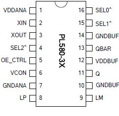
Features: • Less than 0.4ps RMS (12KHz-20MHz) phasejitter for all frequencies.• Less than 25ps (typ.) peak to peak jitter for all frequencies.• Low phase noise output (@ 1MHz frequency offset -144dBc/Hz for 155.52MHz -140dBC/Hz for 311.04MHz• 19MHz-40MHz crystal input.̶...
PL580-38: Features: • Less than 0.4ps RMS (12KHz-20MHz) phasejitter for all frequencies.• Less than 25ps (typ.) peak to peak jitter for all frequencies.• Low phase noise output (@ 1MHz frequ...
SeekIC Buyer Protection PLUS - newly updated for 2013!
268 Transactions
All payment methods are secure and covered by SeekIC Buyer Protection PLUS.
PARAMETERS | SYMBOL | MIN. | MAX. | UNITS |
Supply Voltage | VDD | 4.6 | V | |
Input Voltage, dc | VI | -0.5 | VDD+0.5 | V |
Output Voltage, dc | VO | -0.5 | VDD+0.5 | V |
Storage Temperature | TS | -65 | 150 | |
Ambient Operating Temperature* | TA | -40 | 85 | |
Junction Temperature | TJ | 125 | ||
Lead Temperature (soldering, 10s) | 260 | |||
ESD Protection, Human Body Model | 2 | kV |
Exposure of the device under conditions beyond the limits specified by Maximum Ratings for extended periods may cause permanent damage to the device and affect product reliability. These conditions represent a stress rating only, and functional operations of the device at these or any other conditions above the operational limits noted in this specification is not implied.
* Note: Operating Temperature is guaranteed by design for all parts (COMMERCIAL and INDUSTRIAL), but tested for COMMERCIAL grade only.
The PL580-3X is a monolithic low jitter and low phase noise VCXO, capable of 0.4ps RMS phase jitter and CMOS, LVDS, or PECL outputs, covering a wide frequency output range up to 320MHz. It allows the control of the output frequency with an input voltage (VCON), using a low cost crystal.
The frequency selector pads of PL580-3X enable output frequencies of (2, 4, 8, or 16) * FXIN. The PL580-3X is designed to address the demanding requirements of high performance applications such as SONET, GPS, Video, etc.