PEF3452

Features: • Generic analog interface for all DS3/STS-1/E3applications• Single chip solution for receive and transmit direction• 3.3 V low power device• Integrated receive equalization network• Integrated noise and crosstalk filter• Clock and data recovery using ...

product image

PEF3452 Picture
SeekIC No. : 004459503 Detail

PEF3452: Features: • Generic analog interface for all DS3/STS-1/E3applications• Single chip solution for receive and transmit direction• 3.3 V low power device• Integrated receive equ...

floor Price/Ceiling Price

Part Number:
PEF3452
Supply Ability:
5000

Price Break

  • Qty
  • 1~5000
  • Unit Price
  • Negotiable
  • Processing time
  • 15 Days
Total Cost: $ 0.00

SeekIC Buyer Protection PLUS - newly updated for 2013!

  • Escrow Protection.
  • Guaranteed refunds.
  • Secure payments.
  • Learn more >>

Month Sales

268 Transactions

Rating

evaluate  (4.8 stars)

Upload time: 2024/11/25

Payment Methods

All payment methods are secure and covered by SeekIC Buyer Protection PLUS.

Notice: When you place an order, your payment is made to SeekIC and not to your seller. SeekIC only pays the seller after confirming you have received your order. We will also never share your payment details with your seller.
Product Details

Description


Features:

• Generic analog interface for all DS3/STS-1/E3
applications
• Single chip solution for receive and transmit direction
• 3.3 V low power device
• Integrated receive equalization network
• Integrated noise and crosstalk filter
• Clock and data recovery using an integrated PLL
with ultra-low intrinsic jitter
• Transmit clock duty cycle correction PLL
• No external components required for clock and data
recovery and receive equalizer
• DSX receive line monitor (additional 20 dB gain according to ANSI T1.102)
• Low transmitter output impedances for high transmit return loss
• Disable function of the analog transmit line outputs
• Transmit pulse shaper to fulfill requirements of ANSI T1.404,
Telcordia GR-499-CORE, ANSI T1.102 and ITU-T G.703 (E3)
• Maximum line length up to 1100 ft. (using standard coaxial cable, for example AT&T
728A, 734A or 734D)
• External line length selection (LBO) is not required
• Jitter specifications of GR-499-CORE and ITU-T G.823 are met
• Integrated jitter attenuation PLL and buffer in transmit direction
• Dual or single rail digital inputs and outputs from/to the framer interface
• Selectable line codes (HDB3 (E3), B3ZS (DS3/STS-1), AMI)
• Analog and digital loss of signal detection and indication
• Automatic RDOP/RDON blanking option in case of LOS
• Bipolar violation indication
• Local loop and remote loop for diagnostic purposes
• Insertion of alarm indication signal ("all ones")
• Flexible hardware or software controlled device configuration
• Device power down function
PRELIMINARY
Hardware Interface Mode
• DS3/STS-1 or E3
• Line Coding (E3: HDB3 or AMI; DS3/STS-1: B3ZS or AMI)
• Transmitter disable
• Power down
• Remote loop
• Local loop
• Single/dual rail operation
• Receive clock edge selection
• Transmit clock edge selection
• Transmit "all ones"
• Receive line monitoring mode
• Automatic RDOP/RDON blanking option
• Jitter attenuation
• Loss of signal indication
• Bipolar violation indication
Microprocessor Interface Mode
• Microprocessor bus compatible interface
• Hardware control lines directly accessible
General
• CMOSdevice
• P-MQFP-44-2 package (body size 10 mm × 10 mm, lead pitch 0.8 mm)
• Single power supply: 3.3 V ± 5%
• 5V-tolerant digital input lines
• Temperature range of -40°C to +85°C
• Low power device


Application

• Interface for SONET/DS3 and E3 network equipment
• WANgateways
• CSU/DSU
• Multiplexers
• Digital crossconnect systems
• DS3/STS-1/E3 Test Equipment


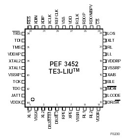
Pinout

  Connection Diagram


Specifications

Parameter

Symbol

Limit Values

Unit

Ambient temperature under bias
TA
40 to 85
°C
Storage temperature
Tstg
65 to 150
°C
IC supply voltage (digital)
VDD
0.4 to 4.5
V
IC supply voltage receive (analog)
VDDR
0.4 to 4.5
V
IC supply voltage transmit (analog)
VDDX
0.4 to 4.5
V
Voltage on any output pin
with respect to ground
VSO
0.4 to 4.5
V
Voltage on any input pin with
respect to ground
VSI
0.4 to 5.5
V
ESD robustness1)
HBM: 1.5 kΩ, 100 pF
V ESD,HBM
2000
V
1) According to MIL-Std 883D, method 3015.7 and ESD Ass. Standard EOS/ESD-5.1-1993.
Note: Stresses above those listed here may cause permanent damage to the
device. Exposure to absolute maximum rating conditions for extended
periods may affect device reliability.


Customers Who Bought This Item Also Bought

Margin,quality,low-cost products with low minimum orders. Secure your online payments with SeekIC Buyer Protection.
Line Protection, Backups
Transformers
Crystals and Oscillators
Programmers, Development Systems
View more