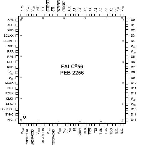
Features: Line Interface
• High-density, generic interface for all E1/T1/J1 applications
• Analog receive and transmit circuits for long-haul and short-haul applications
• E1 or T1/J1 mode selectable
• Data and clock recovery using an integrated digital phase-locked loop
• Maximum line attenuation up to -43 dB at 1024 kHz (E1) and up to -36 dB at 772 kHz (T1/J1)
• Programmable transmit pulse shapes for E1 and T1/J1 pulse masks
• Programmable line build-out for CSU signals according to ANSI T1. 403 and FCC68: 0dB, -7.5dB,
-15dB, -22.5 dB (T1/J1)
• Low transmitter output impedances for high transmit return loss
• Tristate function of the analog transmit line outputs
• Transmit line monitor protecting the device from damage
• Receive line monitor mode
• Jitter specifications of ITU-T I.431, G.703, G.736 (E1), G.823 (E1) and AT&T TR62411 (T1/J1) are met
• Crystal-less wander and jitter attenuation/compensation
• Common master clock reference for E1 and T1/J1 (any frequency within 1.02 and 20 MHz)
• Power-down function
• Support of automatic protection switching
• Dual-rail or single-rail digital inputs and outputs
• Unipolar NRZ or CMI for interfacing fiber-optical transmission routes
• Selectable line codes (E1: HDB3, AMI/T1: B8ZS, AMI with ZCS)
• Loss-of-signal indication with programmable thresholds according to ITU-T G.775,
ETS300233 (E1) and ANSI T1.403 (T1/J1)
• Optional data stream muting upon LOS detection
• Programmable receive slicer threshold
• Clock generator for jitter-free system/transmit clocks per channel
• Local loop and remote loop for diagnostic purposes
• Low power device, single power supply: 3.3 V with 5 V tolerant digital inputs
Frame Aligner
• Frame alignment/synthesis for 2048 kbit/s according to ITU-T G.704 (E1) and for
1544 kbit/s according to ITU-T G.704 and JT G.704 (T1/J1)
• Programmable frame formats:
E1: Doubleframe, CRC multiframe (E1)
T1: 4-frame multiframe (F4,FT), 12-frame multiframe (F12, D3/4), extended
superframe (F24, ESF), remote switch mode (F72, SLC96)
• Selectable conditions for recover/loss of frame alignment
• CRC4 to non-CRC4 interworking according to ITU-T G. 706 Annex B (E1)
• Error checking via CRC4 procedures according to ITU-T G. 706 (E1)
• Error checking via CRC6 procedures according to ITU-T G. 706 and JT G.706 (T1/J1)
• Performs synchronization in ESF format according to NTT requirements (J1)
• Alarm and performance monitoring per second
16 bit counter for CRC-errors, framing errors, code violations, error monitoring via
E-bit and SA6-bit (E1), errored blocks, PRBS bit errors
• Insertion and extraction of alarm indication signals (AIS, remote/yellow alarm,.)
• Remote alarm generation/checking according to ITU JT-G.704 in ESF-format (J1)
• IDLE code insertion for selectable channels
• Single-bit defect insertion
• Flexible system clock frequency for receiver and transmitter
• Supports programmable system data rates with independent receive/transmit shifts:
E1: 2.048, 4.096, 8.192 and 16.384 Mbit/s (according to H.100/H.110 bus)
T1/J1: 2.048, 4.096, 8.192, 16.384 Mbit/s and 1.544, 3.088, 6.176, 12.352 Mbit/s
• Elastic store for receive and transmit route clock wander and jitter compensation;
controlled slip capability and slip indication
• Programmable elastic buffer size: 2 frames/1 frame/short buffer/bypass
• Provides different time slot mapping modes
• Supports fractional E1 or T1/J1 access
• Flexible transparent modes
• Programmable in-band loop code detection and generation (TR62411)
• Channel loop back, line loop back or payload loop back capabilities (TR54016)
• Pseudo-random binary sequence generator and monitor
(framed or unframed)
• Clear channel capabilities (T1/J1)
• Loop-timed mode
Signaling Controller
• Three HDLC controllers
Bit stuffing, CRC check and generation, flag generation, flag and address recognition,
handling of bit oriented functions
• Supports signaling system #7
delimitation, alignment and error detection according to ITU-Q.703
processing of fill in signaling units, processing of errored signaling units
• CAS/CAS-BR controller with last look capability, enhanced CAS-register access and
freeze signaling indication
• DL-channel protocol for ESF format according to ANSI T1.403 specification or
according to AT&T TR54016 (T1/J1)
• DL-bit access for F72 (SLC96) format (T1/J1)
• Generates periodical performance report according to ANSI T1. 403
• Provides access to serial signaling data streams
• Multiframe synchronization and synthesis according to ITU-T G.732
• Alarm insertion and detection (AIS and LOS in time slot 16)
• Transparent mode
• FIFO buffers (64 bytes deep) for efficient transfer of data packets
• Time slot assignment
Any combination of time slots selectable for data transfer independent of signaling
mode (useful for fractional T1/J1 applications)
• Time-slot 0 Sa8...4-bit handling via FIFOs (E1)
• HDLC access to any Sa-bit combination (E1)
Microprocessor Interface
• 8/16-bit microprocessor bus interface (Intel or Motorola type)
• All registers directly accessible (byte or word access)
• Multiplexed and non-multiplexed address bus operations
• Hard/software reset options
• Extended interrupt capabilities
• One-second timer (internal or external timing reference)
General
• Boundary scan standard IEEE 1149.1
• P-LBGA-81-1 package; body size 10 mm * 10 mm; ball pitch 1.0 mm or
• P-MQFP-80-1 package; body size 14 mm * 14 mm; lead pitch 0.5 mm
• Temperature range from -40 to +85 °C
• 3.3 V power supply, digital inputs 5V tolerant
• Typical power consumption 250 mW
Application• Wireless basestations
• E1/T1/J1 ATM gateways, multiplexer
• E1/T1/J1 Channel & Data Service Units (CSU, DSU)
• E1/T1/J1 Internet access equipment
• LAN/WAN router
• ISDN PRI, PABX
• Digital Access Crossconnect Systems (DACS)
• SONET/SDH add/drop multiplexerPinout Specifications
| Parameter |
Symbol |
Limit Values |
Unit |
| Ambient temperature under bias |
TA |
40 to 85 |
°C |
| Storage temperature |
Tstg |
65 to 125 |
°C |
| IC supply voltage (digital) |
VDD |
0.4 to 6.5 |
V |
| IC supply voltage receive (analog) |
VDDR |
0.4 to 6.5 |
V |
| IC supply voltage transmit (analog) |
VDDX |
0.4 to 6.5 |
V |
| Voltage on any pin with respect to ground |
VS |
0.4 to 6.5 |
V |
| ESD robustness1) HBM: 1.5 kΩ, 100 pF |
VESD,HBM |
2000 |
V |
1) According to JEDEC standard JESD22-A114.
Note: Stresses above those listed here may cause permanent damage to the
device. Exposure to absolute maximum rating conditions for extended
periods may affect device reliability.

 PEB2256 Data Sheet


