Features: • Digitally programmable in 256 delay steps
• Monotonic delay-versus-address variation
• Two separate outputs: inverting & non-inverting
• Precise and stable delays
• Input & outputs fully TTL interfaced & buffered
• 10 T2L fan-out capability
• Fits standard 40-pin DIP socket
• Auto-insertableApplicationThe PDU18F is a memory device. As such, special precautions must be taken when changing the delay address in order to prevent spurious output signals. The timing restrictions are shown in Figure 1.
After the last signal edge to be delayed has appeared on the OUT pin, a minimum time, TOAX, is required before the address lines can change.
This time is given by the following relation:
TOAX = max { (Ai - A i-1) * TINC , 0 }
where A i-1 and Ai are the old and new address codes, respectively. Violation of this constraint may, depending on the history of the input signal, cause spurious signals to appear on the OUT pin. The possibility of spurious signals persists until the required TOAX has elapsed.
A similar situation occurs when using the EN/signal to disable the output while IN is active. In this case, the unit must be held in the disabled state until the device is able to "clear" itself. This is achieved by holding the EN/ signal high and the IN signal low for a time given by:
TDISH = Ai * TINC
Violation of this constraint may, depending on the history of the input signal, cause spurious signals to appear on the OUT pin. The possibility of spurious signals persists until the required TDISH has elapsed.
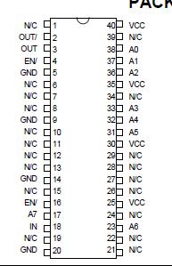
Pinout Specifications
| PARAMETER |
SYMBOL |
MIN |
MAX |
UNITS |
NOTES |
| DC Supply Voltage |
VCC |
-0.3 |
7.0 |
V |
|
| Input Pin Voltage |
VIN |
-0.3 |
VDD+0.3 |
V |
|
| Storage Temperature |
TSTRG |
-55 |
150 |
C |
|
| Lead Temperature |
TLEAD |
|
300 |
C |
10 sec |
DescriptionThe PDU18F-series device is a 8-bit digitally programmable delay line. The delay, TDA, from the input pin (IN) to the output pins (OUT, OUT/) depends on the address code (A7-A0) according to the following formula:
TDA = TD0 + TINC * A
where A is the address code, TINC is the incremental delay of the device, and TD0 is the inherent delay of the PDU18F. The incremental delay is specified by the dash number of the PDU18F and can range from 0.5ns through 10ns, inclusively. The enable pins (EN/) are held LOW during normal operation. These pins must always be in the same state and may be tied together externally. When these signals are brought HIGH, OUT and OUT/ are forced into LOW and HIGH states, respectively. The address is not latched and must remain asserted during normal operation.

 PDU18F Data Sheet


