PD70F3102-33

Features: •µPD703102-33 compatibleCan be replaced by the µPD703102-33 with internal mask ROM for mass production•Internal flash memory: 128 KBPinoutSpecifications Parameter Symbol Conditions Ratings Unit Supply voltagec VDD VDDpin 0.5 to +4.6 V HVDD HVDD...

product image

PD70F3102-33 Picture
SeekIC No. : 004457278 Detail

PD70F3102-33: Features: •µPD703102-33 compatibleCan be replaced by the µPD703102-33 with internal mask ROM for mass production•Internal flash memory: 128 KBPinoutSpecifications Parame...

floor Price/Ceiling Price

Part Number:
PD70F3102-33
Supply Ability:
5000

Price Break

  • Qty
  • 1~5000
  • Unit Price
  • Negotiable
  • Processing time
  • 15 Days
Total Cost: $ 0.00

SeekIC Buyer Protection PLUS - newly updated for 2013!

  • Escrow Protection.
  • Guaranteed refunds.
  • Secure payments.
  • Learn more >>

Month Sales

268 Transactions

Rating

evaluate  (4.8 stars)

Upload time: 2025/1/10

Payment Methods

All payment methods are secure and covered by SeekIC Buyer Protection PLUS.

Notice: When you place an order, your payment is made to SeekIC and not to your seller. SeekIC only pays the seller after confirming you have received your order. We will also never share your payment details with your seller.
Product Details

Description


Features:

•µPD703102-33 compatibleCan be replaced by the µPD703102-33 with internal mask ROM for mass production
•Internal flash memory: 128 KB


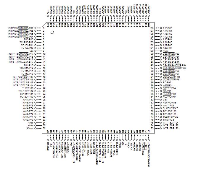
Pinout

  Connection Diagram


Specifications

Parameter Symbol Conditions Ratings Unit
Supply voltagec VDD VDDpin 0.5 to +4.6 V
HVDD HVDDpin, HVDD VDD 0.5 to +7.0 V
CVDD CVDD pin 0.5 to +4.6 V
CVSS CVSSpin 0.5 to +0.5 V
AVDD AVDDpin 0.5 to HVDD+ 0.5 V
AVSS AVSSpin 0.5 to +0.5 V
Input voltage VI Except X1 pin, MODE3/VPPpin 0.5 to HVDD+ 0.5 V
MODE3/VPPpin 0.5 to VDD+ 0.5 V
MODE3/VPPpin in flash memoryprogramming mode 0.5 to +11.0 V
Clock input voltage VK X1, VDD= 3.0 to 3.6 V 0.5 to VDD+ 1.0 V
Output current, low IOL 1 pin 4.0 mA
Total of all pins 100 mA
Output current, high IOH 1 pin 4.0 mA
Total of all pins 100 mA
Output voltage VO HVDD= 5.0 V ±10% 0.5 to HVDD+ 0.5 V
Analog input voltage VIAN P70/ANI0 to
P77/ANI7 pins
AVDD> HVDD 0.5 to HVDD+ 0.5 V
HVDDAVDD 0.5 to AVDD+ 0.5 V
A/D converter reference input
voltage
AVREF AVDD> HVDD 0.5 to HVDD+ 0.5 V
HVDD AVDD 0.5 to AVDD+ 0.5 V
Operating ambient temperature TA   40 to +85 °C
Storage temperature Tstg   65 to +125 °C


Description

The µPD70F3102-33 is a product that substitutes the internal mask ROM of the µPD703102-33 with flashmemory.  This enables users to perform on-board program writing and erasure, enabling effective evaluation duringsystem development, small-lot production of multiple devices, and rapid production start, and quick development andtime-to-market.

A version using a 3.3 V power supply for external pins, the µPD70F3102-33, is also available.

For additional information of PD70F3102-33 , refer to the following user's manuals.  Be sure to read them before startingdesign. V850E/MS1 User's Manual   Hardware:U12688E
V850E/MS1 User's Manual   Architecture:U12197E


Customers Who Bought This Item Also Bought

Margin,quality,low-cost products with low minimum orders. Secure your online payments with SeekIC Buyer Protection.
Optical Inspection Equipment
Discrete Semiconductor Products
Soldering, Desoldering, Rework Products
Power Supplies - Board Mount
View more