Features: . Number of instructions: 74
. Minimum instruction execution time:
58.8 ns (@ 17 MHz operation with main systemclock (fXX))
50 ns (@ 20 MHz operation with main systemclock (fXX))
30.5 µs (@ 32.768 kHz operation with subsystemclock (fXT))
. General-purpose registers: 32 bits × 32 registers
. Instruction set:
Signed multiplication, saturation operations, 32-bit
shift instructions, bit manipulation instructions,
load/store instructions
. Memory space:
16 MB linear address space
Memory block division function: 2 MB per block
. Internal memory
•Flash memory
128 KB (µPD70F3015B, 70F3015BY)
256 KB (µPD70F3017A, 70F3017AY)
•RAM
4 KB (µPD70F3015B, 70F3015BY)
8 KB (µPD70F3017A, 70F3017AY)
. External bus interface: 16-bit data bus
Address bus: Separate output enabled
. Interrupts and exceptions
External: 8, internal: 23, exceptions: 1
. I/O lines Total: 85
. Timer/counters
16-bit timer:2 channels
8-bit timer:4 channels
. Watch timer: 1 channel
. Watchdog timer: 1 channel
. Serial interface (SIO)
Asynchronous serial interface (UART)
Clocked serial interface (CSI)
I2C bus interface (µPD70F3015BY, 70F3017AY)
. A/D converter: 12 channels
. DMA controller: 3 channels
. RTP: 8 bits × 1 channel or 4 bits × 2 channels
. Power-saving functions: HALT/IDLE/STOP modes
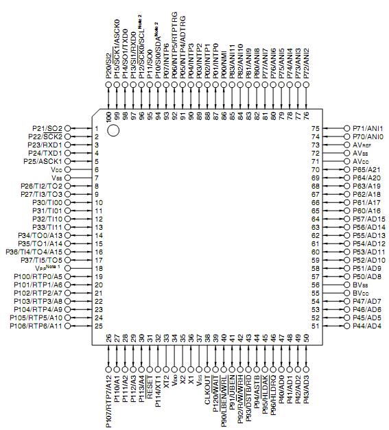
. Packages:100-pin plastic LQFP (14 × 14 mm)
121-pin plastic FBGA (12 × 12 mm)
ApplicationLow-power portable devices
Cellular phones, PHSs, and camcordersPinout Specifications
|
Parameter |
Symbol |
Conditions |
Ratings |
Unit |
|
Supply voltage |
VDD
|
|
0.5 to +4.6 |
V |
|
VPP
|
|
0.5 to +8.5 |
V |
|
AVDD
|
|
0.5 to +4.6 |
V |
|
BVDD
|
|
0.5 to +4.6 |
V |
|
VSS
|
|
0.5 to +0.5 |
V |
|
AVSS
|
|
0.5 to +0.5 |
V |
|
BVSS
|
|
0.5 to +0.5 |
V |
|
Input voltage |
VI1 |
Note 1, P114,RESET
|
0.5 to VDD+ 0.5Note 4
|
V |
|
VI2 |
Note 2 |
0.5 to BVDD+ 0.5Note 4
|
V |
|
Clock input voltage |
VK |
X1, XT1, XT2, VDD= 2.7 to 3.6 V |
0.5 to VDD+ 1.0Note 4
|
V |
|
Analog input voltage |
VIAN |
Note 3(AVDD) |
0.5 to AVDD+ 0.5Note 4
|
V |
|
Analog reference inputvoltage |
AVREF |
AVREF
|
0.5 to AVDD+ 0.5Note 4
|
V |
|
Output current, low |
IOL |
Per pin |
4.0 |
mA |
|
Total for P00 to P07, P10 to P15, P20 to P25 |
25 |
mA |
|
Total for P26, P27, P30 to P37, P100 toP107, P110 to P113 |
25 |
mA |
|
Total for P40 to P47, P90 to P96, P120,CLKOUT |
25 |
mA |
|
Total for P50 to P57, P60 to P65 |
25 |
mA |
|
Output current, high |
IOH |
Per pin |
4.0 |
mA |
|
Total for P00 to P07, P10 to P15, P20 to P25 |
25 |
mA |
|
Total for P26, P27, P30 to P37, P100 toP107, P110 to P113 |
25 |
mA |
|
Total for P40 to P47, P90 to P96, P120,CLKOUT |
25 |
mA |
|
Total for P50 to P57, P60 to P65 |
25 |
mA |
|
Output voltage |
VO1 |
Note 1, VDD= 2.7 to 3.6 V |
0.5 to VDD+ 0.5Note 4
|
V |
|
VO2 |
Note 2, CLKOUT, BVDD= 2.7 to 3.6 V |
0.5 to BVDD+ 0.5Note 4
|
V |
|
Operating ambient temperature |
TA |
Normal operating mode |
40 to +85 |
°C |
|
Flash memory programming mode |
10 to 40 |
°C |
|
Storage temperature |
Tstg |
|
40 to +125
|
°C |
DescriptionThe µPD70F3015B, 70F3015BY, 70F3017A, and 70F3017AY are products with on-chip flash memory. Becausethe devices can be programmed by the user on-board, they are ideal for the evaluation stages of systemdevelopment, small-scale production of a variety of products, and rapiddevelopment of new products.
The PD70F3015B provides a high-level cost performance ideal for applications ranging from low-power camcordersand other AV equipment to portable telephone equipment such as cellular phones and personal handyphonesystems (PHS).
Detailed function descriptions are provided in the following user's manuals. Be sure to read them beforedesigning. PD70F3015B User's Manual Hardware:U12768E
V850 FamilyTM User's Manual Architecture:U10243E

 PD70F3015B Data Sheet


