PCKV857

Features: • ESD classification testing is done to JEDEC Standard JESD22. Protection exceeds 2000 V to HBM per method A114.• Latch-up testing is done to JEDEC Standard JESD78 which exceeds 100 mA• Optimized for clock distribution in DDR (Double Data Rate) SDRAM applications as per...

product image

PCKV857 Picture
SeekIC No. : 004456669 Detail

PCKV857: Features: • ESD classification testing is done to JEDEC Standard JESD22. Protection exceeds 2000 V to HBM per method A114.• Latch-up testing is done to JEDEC Standard JESD78 which exceed...

floor Price/Ceiling Price

Part Number:
PCKV857
Supply Ability:
5000

Price Break

  • Qty
  • 1~5000
  • Unit Price
  • Negotiable
  • Processing time
  • 15 Days
Total Cost: $ 0.00

SeekIC Buyer Protection PLUS - newly updated for 2013!

  • Escrow Protection.
  • Guaranteed refunds.
  • Secure payments.
  • Learn more >>

Month Sales

268 Transactions

Rating

evaluate  (4.8 stars)

Upload time: 2025/1/6

Payment Methods

All payment methods are secure and covered by SeekIC Buyer Protection PLUS.

Notice: When you place an order, your payment is made to SeekIC and not to your seller. SeekIC only pays the seller after confirming you have received your order. We will also never share your payment details with your seller.
Product Details

Description


Features:

• ESD classification testing is done to JEDEC Standard JESD22. Protection exceeds 2000 V to HBM per method A114.
• Latch-up testing is done to JEDEC Standard JESD78 which exceeds 100 mA
• Optimized for clock distribution in DDR (Double Data Rate) SDRAM applications as per JEDEC specifications
• 1-to-10 differential clock distribution
• Very low skew (< 100 ps) and jitter (< 100 ps)
• Operation from 2.2 V to 2.7 V AVDD and 2.3 V to 2.7 V VDD
• SSTL_2 interface clock inputs and outputs
• CMOS control signal input
• Test mode enables buffers while disabling PLL
• Low current power-down mode
• Tolerant of Spread Spectrum input clock
• Full DDR solution provided when used with SSTL16877 or SSTV16857
• See PCKV856 for I2C capable clock driver


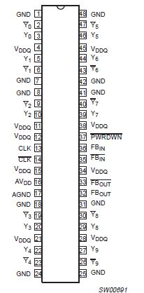
Pinout

  Connection Diagram


Specifications

SYMBOL
PARAMETER
CONDITION
LIMITS
UNIT
MIN
MAX
VDDQ
Supply voltage range
0.5
3.6
V
AVDD
Supply voltage range
0.5
3.6
V
VI
Input voltage range
see Notes 2 and 3
0.5
VDDQ + 0.5
V
VO
Output voltage range
see Notes 2 and 3
-0.5
VDDQ + 0.5
V
IIK
Input clamp current
VI < 0 or VI >VDDQ
-
±50
mA
IOK
Output clamp current
VO < 0 or VO >VDDQ
-
±50
mA
IO
Continuous output current
VO = 0 to VDDQ
±50
mA
Continuous current to GND or VDDQ
-
±100
mA
Ptot
Storage temperature range
-65
+150
°C

NOTES:
1. Stresses beyond those listed may cause permanent damage to the device. These are stress ratings only and functional operation of the device at these or any other conditions beyond those indicated under "recommended operating conditions" is not implied. Exposure to absolute-maximum-rated conditions for extended periods may affect device reliability.
2. The input and output voltage ratings may be exceeded if the input and output current ratings are observed.
3. This value is limited to 3.6 V maximum.


Description

The PCKV857 is a high-performance, low-skew, low-jitter zero delay buffer designed for 2.5 V VDD and 2.5 V AVDD operation and differential data input and output levels.

The PCKV857 is a zero delay buffer that distributes a differential clock input pair (CLK, CLK) to ten differential pairs of clock outputs (Y[0:9], Y[0:9]) and one differential pair feedback clock outputs (FBOUT,  FBOUT) . The clock outputs are controlled by the clock inputs (CLK, CLK), the feedback clocks (FBIN,  FBIN), and the analog power input (AVDD). When  PWRDWN of PCKV857 is high, the outputs switch in phase and frequency with CLK. When  PWRDWN is low, all outputs are disabled to high impedance state (3-State), and the PLL is shut down (low power mode). The device also enters the low power mode when the input frequency falls below 20 MHz. An input frequency detection circuit will detect the low frequency condition and after applying a > 20 MHz input signal, the detection circuit turns on the PLL again and enables the outputs. When AVDD is grounded, the PLL is turned off and bypassed for test purposes. The PCKV857 is also able to track spread spectrum clocking for reduced EMI.

The PCKV857 is characterized for operation from 0 to +70 °C.


Customers Who Bought This Item Also Bought

Margin,quality,low-cost products with low minimum orders. Secure your online payments with SeekIC Buyer Protection.
Discrete Semiconductor Products
Connectors, Interconnects
Static Control, ESD, Clean Room Products
Power Supplies - External/Internal (Off-Board)
Sensors, Transducers
Integrated Circuits (ICs)
View more