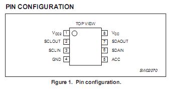
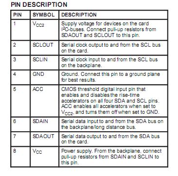
Features: Bi-directional buffer for SDA and SCL lines increases fanout andprevents SDA and SCL corruption during live board insertion andremoval from multi-point backplane systemsCompatible with I2 C standard mode, I 2C fast mode, and SMBus standardst rise time accelerators on all SDA and SCL line...
PCA9512: Features: Bi-directional buffer for SDA and SCL lines increases fanout andprevents SDA and SCL corruption during live board insertion andremoval from multi-point backplane systemsCompatible with I2 ...
SeekIC Buyer Protection PLUS - newly updated for 2013!
268 Transactions
All payment methods are secure and covered by SeekIC Buyer Protection PLUS.
Bi-directional buffer for SDA and SCL lines increases fanout and
prevents SDA and SCL corruption during live board insertion and
removal from multi-point backplane systems
Compatible with I2 C standard mode, I 2C fast mode, and SMBus standardst
rise time accelerators on all SDA and SCL lines with ability to disable rise time accelerators through the ACC pin for
lightly loaded systems5 V to 3.3 V level translation with optimum noise margin
High-impedance SDA, SCL pins for V or VCC = 0 Vcc
precharge on all SDA and SCL linesSupports clock stretching and multiple master arbitration/synchronization
Operating power supply voltage range: 2.7 V to 5.5 V5.5 V tolerant I/Os0 kHz to 400 kHz clock frequencyESD protection exceeds 2000 V HBM per JESD22-A114,
200 V MM per JESD22-A115 and 1000 V CDM per JESD22-C101
Latch-up testing is done to JESDEC Standard JESD78 which
exceeds 100 mAPackages offered: SO8, TSSOP8 (MSOP8)
symbol | partameter | conditions | RATING | unit | |
MIN | MAX | ||||
VCC |
Supply voltage range VCC |
-0.5 | +7 | V | |
VCC2 |
Supply voltage range VCC2 | -0.5 | +7 | V | |
Vn | SDAIN, SCLIN, SDAOUT, SCLOUT, ACC | -0.5 | +7 | V | |
PI |
Maximum current for inputs | - | ±20 | MA | |
IIO | Maximum current for I/O pins | - | ±50 | MA | |
Topr | Operating temperature range | -40 | +85 | °C | |
Tstg | Storage temperature range | -65 | +125 | °C | |
Tsld | Lead soldering temperature (10 sec max) | - | +300 | °C | |
Tj(max) | Maximum junction temperature | - | +125 | °C |
The PCA9512 is a hot swappable I2C and SMBus buffer that allows I/O card insertion into a live backplane without corruption of the data and clock buses and includes two dedicated supply voltage pins to provide level shifting between 3.3 V and 5 V systems while maintaining the best noise margin for each voltage level. Either pin of PCA9512 may be powered with supply voltages ranging from 2.7 V to 5.5 V with no constraints on which supply voltage is higher. Control circuitry prevents the backplane from being connected to the card until a stop bit or bus idle occurs on the backplane without bus contention on the card. When the connection is made, the PCA9512 provides bi-directional buffering, keeping the backplane and card capacitances isolated.
The dynamic offset design of the PCA9510/11/12/13/14 I/O drivers allow them to be connected to another PCA9510/11/12/13/14 device in series or in parallel and to the A side of the PCA9517. ThePCA9510/11/12/13/14 can not connect to the static offset I/Os usedon the PCA9515/15A/16/16A/17 B side and PCA9518.