OPA656

Features: 500MHz UNITY-GAIN BANDWIDTH LOW INPUT BIAS CURRENT: 2pA LOW OFFSET AND DRIFT: ±0.25mV, ±2V/°C LOW DISTORTION: 74dB SFDR at 5MHz HIGH OUTPUT CURRENT: 70mA LOW INPUT VOLTAGE NOISE: 7nV/HzApplicationWIDEBAND PHOTODIODE AMPLIFIERSSAMPLE-AND-HOLD BUFFERS CCD OUTPUT BUFFERSADC INPUT BUFFERS WI...

product image

OPA656 Picture
SeekIC No. : 004438438 Detail

OPA656: Features: 500MHz UNITY-GAIN BANDWIDTH LOW INPUT BIAS CURRENT: 2pA LOW OFFSET AND DRIFT: ±0.25mV, ±2V/°C LOW DISTORTION: 74dB SFDR at 5MHz HIGH OUTPUT CURRENT: 70mA LOW INPUT VOLTAGE NOISE: 7nV/HzApp...

floor Price/Ceiling Price

Part Number:
OPA656
Supply Ability:
5000

Price Break

  • Qty
  • 1~5000
  • Unit Price
  • Negotiable
  • Processing time
  • 15 Days
Total Cost: $ 0.00

SeekIC Buyer Protection PLUS - newly updated for 2013!

  • Escrow Protection.
  • Guaranteed refunds.
  • Secure payments.
  • Learn more >>

Month Sales

268 Transactions

Rating

evaluate  (4.8 stars)

Upload time: 2024/11/21

Payment Methods

All payment methods are secure and covered by SeekIC Buyer Protection PLUS.

Notice: When you place an order, your payment is made to SeekIC and not to your seller. SeekIC only pays the seller after confirming you have received your order. We will also never share your payment details with your seller.
Product Details

Description


Features:

500MHz UNITY-GAIN BANDWIDTH
LOW INPUT BIAS CURRENT: 2pA
LOW OFFSET AND DRIFT: ±0.25mV, ±2V/°C
LOW DISTORTION: 74dB SFDR at 5MHz
HIGH OUTPUT CURRENT: 70mA
LOW INPUT VOLTAGE NOISE: 7nV/Hz


Application

 WIDEBAND PHOTODIODE AMPLIFIERS
SAMPLE-AND-HOLD BUFFERS
CCD OUTPUT BUFFERS
ADC INPUT BUFFERS
WIDEBAND PRECISION AMPLIFIERS
TEST AND MEASUREMENT FRONT ENDS


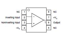
Pinout

  Connection Diagram


Specifications

Supply Voltage ................................................................................ ±6.5V
Internal Power Dissipation ........................... See Thermal Characteristics
Differential Input Voltage .................................................................. ±VS
Input Voltage Range ......................................................................... ±VS
Storage Temperature Range .................................... 40°C to +125°C
Lead Temperature ..................................................................... +260°C
Junction Temperature (TJ ) ........................................................ +150°C
ESD Rating (Human Body Model) .................................................. 2000V
                  (Machine Model) ............................................................ 200V
NOTE: (1) Stresses above these ratings may cause permanent damage.
Exposure to absolute maximum conditions for extended periods may degrade
device reliability. These are stress ratings only, and functional operation of the
device at these or any other conditions beyond those specified is not implied.


Description

The OPA656 combines a very wideband, unity-gain stable, voltage-feedback op amp with a FET-input stage to offer an ultra high dynamic-range amplifier for ADC (Analog-to-Digital Converter) buffering and transimpedance applications. Extremely low DC errors give good precision in optical applications.

The high unity-gain stable bandwidth and JFET input allows exceptional performance in high-speed, low-noise integrators. The high input impedance and low bias current provided by the FET input is supported by the ultra-low 7nV/Hz input voltage noise to achieve a very low integrated noise in wideband photodiode transimpedance applications.

Broad transimpedance bandwidths are achievable given the OPA656's high 230MHz gain bandwidth product. As shown below, a 3dB bandwidth of 1MHz is provided even for a high 1MW transimpedance gain from a 47pF source capacitance.


Customers Who Bought This Item Also Bought

Margin,quality,low-cost products with low minimum orders. Secure your online payments with SeekIC Buyer Protection.
Boxes, Enclosures, Racks
Cables, Wires
Programmers, Development Systems
Semiconductor Modules
Crystals and Oscillators
View more