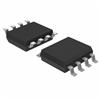
DescriptionThe OPA343NA is designed as rail-to-rail CMOS operational amplifier for low cost, miniature applications. It is optimized for low voltage, single supply operation. Rail-to-rail input/output and high speed operation make them ideal for driving sampling analogto-digital converters.OPA343N...
OPA343NA: DescriptionThe OPA343NA is designed as rail-to-rail CMOS operational amplifier for low cost, miniature applications. It is optimized for low voltage, single supply operation. Rail-to-rail input/outp...
SeekIC Buyer Protection PLUS - newly updated for 2013!
268 Transactions
All payment methods are secure and covered by SeekIC Buyer Protection PLUS.
US $.5 - .51 / Piece
Operational Amplifiers - Op Amps Hi-Speed Low Noise Single Supply CMOS
The OPA343NA is designed as rail-to-rail CMOS operational amplifier for low cost, miniature applications. It is optimized for low voltage, single supply operation. Rail-to-rail input/output and high speed operation make them ideal for driving sampling analogto-digital converters.
OPA343NA has eight features. (1)Rail to rail input. (2)Rail to rail output (within 1mV). (3)Microsize packages. (4)Wide bandwidth 5.5MHz. (5)High slew rate 6V/us. (6)Low THD+noise 0.0007% (f=1kHz). (7)Low quiescent current 850uA/channel. (8)Single, dual and quad. Those are all the main features.
Some absolute maximum ratings of OPA343NA have been concluded into several points as follow. (1)Its supply voltage is 5.5V. (2)Its signal input terminals voltage would be from V- -0.5V to V+ +0.5V. (3)Its single input terminals current would be 10mA. (4)Its output short-circuit would be continuous. (5)Its operating temperature range would be from -55°C to +125°C. (6)Its storage temperature range would be from -55°C to +125°C. (7)Its junction temperature would be 150°C. (8)Its lead temperature (soldering 10s) would be 300°C. It should be noted that stresses above those listed in absolute maximum ratings may cause permanent damage to device.
Also some electrical characteristics of OPA343NA are concluded as follow. (1)Its input offset voltage would be typ +/-2mV and max +/-8mV. (2)Its channel separation would be typ 0.2uV/V. (3)Its input bias current would be typ +/0.2pA and max +/-10pA. (4)Its input offset current would be typ +/-0.2pA and max +/-10pA. (5)Its input voltage noise f=0.1 to 50kHz would be typ 8uVrms. (6)Its input voltage noise density f=1kHz would be typ 25nV/Hz. (7)Its common mode voltage range would be from -0.3V to V+ +0.3V. (8)Its common -mode rejection ratio would be min 74dB and typ 92dB. (9)Its gain-bandwidth product would be typ 5.5MHz. (10)Its slew rate would be typ 6V/us. And so on. If you have any question or suggestion or want to know more information please contact us for details. Thank you!