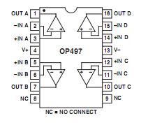
Features: Low Offset Voltage: 50 V max
Low Offset Voltage Drift: 0.5 V/ max
Very Low Bias Current
25: 100 pA max
55 to +125: 450 pA max
Very High Open-Loop Gain: 2000 V/mV min
Low Supply Current (per Amplifier): 625 A max
Operates from ±2 V to ±20 V Supplies
High Common-Mode Rejection: 120 dB minApplicationStrain Gage and Bridge Amplifiers
High Stability Thermocouple Amplifiers
Instrumentation Amplifiers
Photo-Current Monitors
High Gain Linearity Amplifiers
Long-Term Integrators/Filters
Sample-and-Hold Amplifiers
Peak Detectors
Logarithmic Amplifiers
Battery-Powered SystemsPinout SpecificationsSupply Voltage . . . . . . . . . . . . . . . . . . . . . . . . . . . . . . . . ±20 V
Input Voltage2. . . . . . . . . . . . . . . . . . . . . . . . . . . . . . . . . . 20 V
Differential Input Voltage2. . . . . . . . . . . . . . . . . . . . . . . . . 40 V
Output Short-Circuit Duration . . . . . . . . . . . . . . . . Indefinite
Storage Temperature Range
Y Package . . . . . . . . . . . . . . . . . . . . . . . . 65°C to +175°C
P, S Package . . . . . . . . . . . . . . . . . . . . . . . 65°C to +150°C
Operating Temperature Range
OP497A, C (Y) . . . . . . . . . . . . . . . . . . . .. 55°C to +125°C
OP497F, G (Y) . . . . . . . . . . . . . . . . . . . . .. 40°C to +85°C
OP497F, G (P, S) . . . . . . . . . . . . . . . . . . .. 40°C to +85°C
Junction Temperature
Y Package . . . . . . . . . . . . . . . . . . . . . . . . 65°C to +175°C
P, S Package . . . . . . . . . . . . . . . . . . . . . . .65°C to +150°C
Lead Temperature Range (Soldering 60 sec) . . . . . . . .300°C
| -3dB Bandwidth |
500kHz |
| Slew Rate |
150mV/s |
| Vos |
80V |
| Ib |
60pA |
| Input Noise (nV/rtHz) |
25nV/rtHz |
| Vcc-Vee Supply (V) |
4 to 40 |
| Iq per Amplifier |
625A |
| # OpAmps per Pkg |
4 |
| Operating Temp Range |
-55 to +125 |
| Packages |
DIP,LCC,SOIC |
DescriptionThe OP497 is a quad op amp with precision performance in the space-saving, industry standard 16-lead SOlC pack-age. Its combination of exceptional precision with low power and extremely low input bias current makes the quad OP497 useful in a wide variety of applications.
Precision performance of the OP497 includes very low offset, under 50 µV, and low drift, below 0.5 µV/°C. Open-loop gain exceeds 2000 V/mV ensuring high linearity in every application. Errors due to common-mode signals are elimin-ated by the OP497's common-mode rejection of over 120 dB. The OP497's power supply rejection of over 120 dB minimizes offset voltage changes experienced in battery-powered systems. Supply current of the OP497 is under 625 µA per amplifier, and it can operate with supply voltages as low as ±2 V.
The OP497 utilizes a superbeta input stage with bias current cancellation to maintain picoamp bias currents at all temperatures. This is in contrast to FET input op amps whose bias currents start in the picoamp range at 25°C, but double for every 10°C rise in temperature, to reach the nanoamp range above 85°C. Input bias current of the OP-497 is under 100 pA at 25°C and is under 450pA over the military temperature range.
Combining precision, low power, and low bias current, the OP497 is ideal for a number of applications, including in-stru mentation amplifiers, log amplifiers, photo-diode preamplifiers, and long-term integrators. For a single device, see the OP97; for a dual device, see the OP297.

 OP497 Data Sheet


