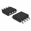
OP215

Features: High Slew Rate: 10 V/s MinFast Settling Time: 0.9 s to 0.1% TypeLow Input Offset Voltage Drift: 10 V/ MaxWide Bandwidth: 3.5 MHz MinTemperature-Compensated Input Bias CurrentsGuaranteed Input Bias Current: 18 nA Max (125)Bias Current Specified Warmed Up over TemperatureLow Input Noise Cu...

product image

OP215 Picture
SeekIC No. : 004437891 Detail

OP215: Features: High Slew Rate: 10 V/s MinFast Settling Time: 0.9 s to 0.1% TypeLow Input Offset Voltage Drift: 10 V/ MaxWide Bandwidth: 3.5 MHz MinTemperature-Compensated Input Bias CurrentsGuaranteed In...

floor Price/Ceiling Price

Part Number:
OP215
Supply Ability:
5000

Price Break

  • Qty
  • 1~5000
  • Unit Price
  • Negotiable
  • Processing time
  • 15 Days
Total Cost: $ 0.00

SeekIC Buyer Protection PLUS - newly updated for 2013!

  • Escrow Protection.
  • Guaranteed refunds.
  • Secure payments.
  • Learn more >>

Month Sales

268 Transactions

Rating

evaluate  (4.8 stars)

Upload time: 2024/11/12

Payment Methods

All payment methods are secure and covered by SeekIC Buyer Protection PLUS.

Notice: When you place an order, your payment is made to SeekIC and not to your seller. SeekIC only pays the seller after confirming you have received your order. We will also never share your payment details with your seller.
Product Details

Description


Features:

High Slew Rate: 10 V/s Min
Fast Settling Time: 0.9 s to 0.1% Type
Low Input Offset Voltage Drift: 10 V/ Max
Wide Bandwidth: 3.5 MHz Min
Temperature-Compensated Input Bias Currents
Guaranteed Input Bias Current: 18 nA Max (125)
Bias Current Specified Warmed Up over Temperature
Low Input Noise Current: 0.01 pA/÷Hz Type
High Common-Mode Rejection Ratio 86 dB Min
Pin Compatible with Standard Dual Pinouts
Models with MIL-STD-883 Class B Processing Available


Specifications

OP215E, OP215G . . . . . . . . . . . . . . . . . . . . . . . . . ±18 V
Operating Temperature Range
OP215E . . . . . . . . . . . . . . . . . . . . . . . . . . . +0 to +70
OP215G . . . . . . . . . . . . . . . . . . . . . . . . . . 40 to +85
Maximum Junction Temperature (Tj) . . . . . . . . . . . . 150
Differential Input Voltage
OP215E . . . . . . . . . . . . . . . . . . . . . . . . . . . . . . . . . ±40 V
OP215G . . . . . . . . . . . . . . . . . . . . . . . . . . . . . . . . . .±30 V
Input Voltage2
OP215E . . . . . . . . . . . . . . . . . . . . . . . . . . . . . . . . . .±20 V
OP215G . . . . . . . . . . . . . . . . . . . . . . . . . . . . . . . . . .±16 V
Output Short-Circuit Duration . . . . . . . . . . . . . . Indefinite
Storage Temperature Range . . . . . . . . . . . . 65 to +150
Lead Temperature (Soldering, 60 sec) . . . . . . . . . . . . . 300
Junction Temperature (Tj) . . . . . . . . . . . . . 65 to +150


Description

The OP215 offers the proven JFET-input performance advantages of high speed and low input bias current with the tracking and convenience advantages of a dual op amp configuration.

Low input offset voltages, low input currents, and low drift are featured in these high-speed amplifiers OP215.

On-chip zener-zap trimming is used to achieve low VOS, while a bias-current compensation scheme gives a low input bias current at elevated temperature. Thus, the OP215 features an input bias current of 1.4 nA at 70C ambient (not junction) temperature which greatly extends the application usefulness of this device.

OP215 Applications include high-speed amplifiers for current output DACs, active filters, sample-and-hold buffers, and photo-cell amplifiers. For additional precision JFET op amps, see the OP249 and AD712 data sheets.


Customers Who Bought This Item Also Bought

Margin,quality,low-cost products with low minimum orders. Secure your online payments with SeekIC Buyer Protection.
RF and RFID
Boxes, Enclosures, Racks
Sensors, Transducers
Test Equipment
View more