Maximum Operating Temperature
: + 85 C
Wavelength
: 880 nm
Packaging
: Reel
Minimum Operating Temperature
: - 25 C
Package / Case
: 0805
Beam Angle
: 100 deg
Radiant Intensity
: 3 mW/sr
Features: Low Input Offset Voltage: 75 V Max
Low Offset Voltage Drift, Over 55 < TA < +125:
0.5 V/ Max
Low Supply Current (Per Amplifier): 725 A Max
High Open-Loop Gain: 5000 V/mV Min
Low Input Bias Current: 2 nA Max
Low Noise Voltage Density: 11 nV/÷Hz at 1 kHz
Stable with Large Capacitive Loads: 10 nF Typ
Pin Compatible to OP221, MC1458, and LT1013 with
Improved Performance
Available in Die FormPinout Specifications
| -3dB Bandwidth |
500kHz |
| Slew Rate |
150mV/s |
| Vos |
80V |
| Ib |
100pA |
| Input Noise (nV/rtHz) |
11nV/rtHz |
| Vcc-Vee Supply (V) |
6 to 40 |
| Iq per Amplifier |
775A |
| # OpAmps per Pkg |
2 |
| Operating Temp Range |
-55 to +125 |
| Packages |
DIP,LCC,SOIC |
Supply Voltage . . . . . . . . . . . . . . . . . . . . . . . . . .±20 V
Differential Input Voltage . . . . . . . . . . . . . . . . . .±30 V
Input Voltage . . . . . . . . . . . . . . . . . . . .Supply Voltage
Output Short-Circuit Duration . . . . . . . . . . Continuous
Storage Temperature Range
P, S, Z-Package . . . . . . . . . . . . . . . . . 65 to +150
Lead Temperature Range (Soldering, 60 sec) . . 300
Junction Temperature (TJ) . . . . . . . . . 65 to +150
Operating Temperature Range
OP200A . . . . . . . . . . . . . . . . . . . . . . . .55 to +125
OP200E, OP200F . . . . . . . . . . . . . . . . . . 40to +85
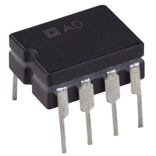
OP200G . . . . . . . . . . . . . . . . . . . . . . . . .40 to +85DescriptionThe OP200 is the first monolithic dual operational amplifier to offer OP77 type precision performance. Available in the industry standard 8-pin pinout, the OP200 combines precision performance with the space and cost savings offered by a dual amplifier.
The OP200 features an extremely low input offset voltage of less than 75 mV with a drift below 0.5 mV/ guaranteed over the full military temperature range. Open-loop gain of the OP200 exceeds 5,000,000 into a 10 kW load; input bias current is under 2 nA; CMR is over 120 dB and PSRR below 1.8 mV/V. On-chip zenerzap trimming is used to ach-ieve the extremely low input offset voltage of the OP200 and eliminates the need for offset pulling.
Power consumption of the OP200 is very low, with each amplifier drawing less than 725 mA of supply current. The total current drawn by the dual OP200 is less than one-half that of a single OP07, yet the OP200 offers significant improvements over this industry standard op amp. The voltage noise density of the OP200, 11 nV/÷Hz at 1 kHz, is half that of most competitive devices.
The OP200 is pin compatible with the OP221, LM158,MC1458/1558, and LT1013.
Parameters: | Technical/Catalog Information | OP200 |
| Vendor | TT Electronics/Optek Technology (VA) |
| Category | Optoelectronics |
| Voltage - Forward (Vf) Typ | 1.6V |
| Current - DC Forward (If) | 100mA |
| Wavelength | 880nm |
| Viewing Angle | 150° |
| Radiant Intensity (Ie) Min @ If | - |
| Mounting Type | Surface Mount |
| Package / Case | Non-Standard SMD |
| Orientation | Top View |
| Packaging | Cut Tape (CT) |
| Lead Free Status | Lead Free |
| RoHS Status | RoHS Compliant |
| Other Names | OP200
OP200
365 1147 1 ND
36511471ND
365-1147-1
|

 OP200 Data Sheet


