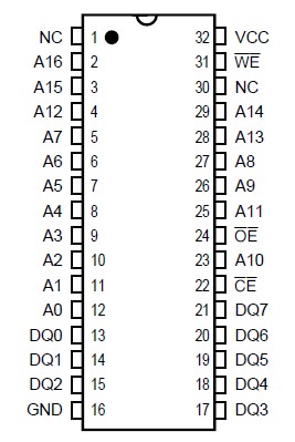
Features: • Ultra-fast Performance
35, 45, 55, 70, and 90 ns max. access times
• Temperature Ranges
Commercial 0oc-70oc
Industrial -40oc-85oc
• Single 5V-only Power Supply
5V ± 10% for Read, Program, and Erase
• CMOS Low Power Consumption
20 mA (typical) active read current
30 mA (typical) Program/Erase current
• Compatible with JEDEC-Standard Pinouts
32-pin DIP, PLCC, TSOP
• Program/function Compatible with AM29F010
No system firmware changes
Uses same PROM programer algorithm
• Flexible sector architecture
Erase any of eight uniform sectors or full chip erase
Sector protection/unprotection using PROM programming equipment
• 100,000 Program/Erase cycles
• Embedded algorithms
Automatically programs and verifies data at specified address
Auto-programs and erases the chip or any designated sector
• Data/Polling and Toggle Bits
Detect program or erase cycle completionPinout Specifications
| Symbol Parameter Value Unit |
VTERM Terminal Voltage with Respect to GND
Any Pin Except A9 2.0 to +7.0(2) V
A9 2.0 to +12.5(2) V
VCC 2.0 to +7.0(2) V |
| ISC Output Short Circuit Current (Max. Limit) 200 mA |
| TA Commercial Operating Temperature 0 to +70 °C |
| TA Industrial Operating Temperature 40 to +85 °C |
| TSTG Storage Temperature 65 to +125 °C |
Notes:
1. Stress greater than those listed under ABSOLUTE MAXIMUM RATINGS may cause permanent damage to the device. This is a stress rating only and functional operation of the device at these or any other conditions above those indicated in the operational sections of this specification is not implied. Exposure to absolute maximum rating conditions for extended periods may affect reliability.
2. Minimum DC inputs, I/O, and A9 pins voltage is 0.5V. During transitions, inputs may undershoot to 2.0V for periods less than 20 ns. Maximum DC voltage on output pins is Vcc + 0.5V, which may overshoot to Vcc + 2.0V for periods less than 20 ns. Maximum DC voltage on A9 is +12.5V that may overshoot to +12.5V for periods less than 20 ns.
3. No more than one output shorted at one time. Duration of short shall not exceed one second.
DescriptionThe NexFlash NX29F010 is a 1 Megabit (131,072 bytes) single 5.0V-only Sectored Flash Memory. The NX29F010 provides in-system programming with the standard system 5.0V-only Vcc supply and can be programmed or erased in standard PROM programmers.
The NX29F010 offers access times of 35, 45, 55, 70, and 90 ns allowing high-speed controller and DSPs' to operate without wait states. Byte-wide data appears on DQ0-DQ7. Separate chip enable (CE), write enable (WE), and output enable (OE) controls eliminates bus contention.
Power consumption is greatly reduced when the system places the NX29F010 into the Standby Mode.
The NX29F010 is offered in 32-pin PLCC, TSOP, and PDIP packages.
Executing the Erase Command Sequence invokes the Embedded Erase Algorithm, an internal algorithm that automatically pre-programs the array to all zeros (if it is not already programmed) before executing the erase operation. During erase, the NX29F010 automatically times the erase pulse widths and verifies proper cell margin during erase.
By reading the DQ7 (Data Polling) and DQ6 (toggle) status bits, the host system can detect whether a program or erase operation is complete. After completion, the NX29F010 is ready to read array data or accept another command.
The sector erase architecture is designed to allow memory sectors to be erased and reprogrammed without affectingthe data contents of other sectors. The NX29F010 is erased before it is shipped to customers.
The hardware data protection includes a low Vcc detector that automatically inhibits write operations during power transitions. The hardware sector protection feature will disable both program and erase operations in any combination of the sectors of memory, and is implemented using standard EPROM programming algorithm. The NX29F010 electrically erases all bits within a sector simultaneously via Fowler-Nordheim tunneling. Data are programmed one byte at a time using the EPROM programming algorithm of hot electron injection.

 NX29F010 Data Sheet


