Pinout Specifications
|
Symbol |
Parameter |
Pin No. |
Min. |
Max. |
Unit |
|
TA |
Ambient Operating
Temperature |
|
0 |
65 |
°C |
|
TS |
Storage Temperature |
|
40 |
+125* |
°C |
|
VSUP |
Supply Voltage |
8 |
0.5 |
+6 |
V |
|
VI |
Input Voltage |
2 to 7 |
0.3 V |
VSUP |
|
|
IO |
Output Current |
7 |
|
5 |
mA |
* Stored data may be affected by TS above +85 °CDescriptionThe INTERMETALL Bus (IM Bus for short) NVM 3060 has been designed to control the DIGIT 2000 ICs by the CCU Central Control Unit. Via this bus the CCU can write data to the ICs or read data from them. This means the CCU acts as a master whereas all controlled ICs are slaves.
The IM Bus NVM 3060 consists of three lines for the signals Ident (ID), Clock (CL) and Data (D). The clock frequency range is 50 Hz to 170 kHz. Ident and clock are unidirectional from the CCU to the slave ICs, Data is bidirectional. Bidirectionality is achieved by using open-drain outputs with On-resistances of 150
maximum. The 2.5 k
pull-up resistor of NVM 3060 common to all outputs is incorporate in the CCU.
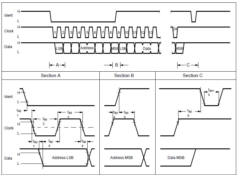
The timing of a complete IM Bus NVM 3060 transaction is shown in Fig. 51. In The non-operative state the signals of all three bus lines are High. To start a transaction the CCU sets the ID signal to Low level, indicating an address transmission, and sets the CL signal to Low level as well to switch the first bit on the Data line. Thereafter eight address bits of NVM 3060 are transmitted beginning with the LSB. Data takeover in the slave ICs occurs at the positive edge of the clock signal. At the end of the address byte the ID signal goes High, initiating the address comparison in the slave circuits. In the addressed slave the IM bus NVM 3060 interface switches over to Data read or write, because these functions are correlated to the address.
Also controlled by the address the CCU now transmits eight or sixteen clock pulses, and accordingly one or two bytes of data are written into the addressed IC or read out from it, eginning with the LSB.
The completion of the bus transaction NVM 3060 is signalled by a short Low-state pulse of the ID signal. This initiates the storing of the transferred data.
NVM 3060 is permissible to interrupt a bus transaction for up to 10 ms.

 NVM 3060 Data Sheet


