NTE955MC

Features: · Direct Replacement for 555 Timers· Very Low Power Consumption: 1mW Typ at VDD = 5V· Operates in Both Astable and Monostable Modes· CMOS Output Capable of Swinging Rail to Rail· High Output Current Capability: Sink 100mA Typ Source 10mA Typ· Output Fully Compatible with CMOS, TTL, and M...

product image

NTE955MC Picture
SeekIC No. : 004436607 Detail

NTE955MC: Features: · Direct Replacement for 555 Timers· Very Low Power Consumption: 1mW Typ at VDD = 5V· Operates in Both Astable and Monostable Modes· CMOS Output Capable of Swinging Rail to Rail· High Outp...

floor Price/Ceiling Price

Part Number:
NTE955MC
Supply Ability:
5000

Price Break

  • Qty
  • 1~5000
  • Unit Price
  • Negotiable
  • Processing time
  • 15 Days
Total Cost: $ 0.00

SeekIC Buyer Protection PLUS - newly updated for 2013!

  • Escrow Protection.
  • Guaranteed refunds.
  • Secure payments.
  • Learn more >>

Month Sales

268 Transactions

Rating

evaluate  (4.8 stars)

Upload time: 2025/1/8

Payment Methods

All payment methods are secure and covered by SeekIC Buyer Protection PLUS.

Notice: When you place an order, your payment is made to SeekIC and not to your seller. SeekIC only pays the seller after confirming you have received your order. We will also never share your payment details with your seller.
Product Details

Description


Features:

· Direct Replacement for 555 Timers
· Very Low Power Consumption: 1mW Typ at VDD = 5V
· Operates in Both Astable and Monostable Modes
· CMOS Output Capable of Swinging Rail to Rail
· High Output Current Capability: Sink 100mA Typ Source 10mA Typ
· Output Fully Compatible with CMOS, TTL, and MOS
· Low Supply Current Reduces Spikes During Output Transitions
· Single Supply Operation from 2V to 15V


Application

· Precision Timing
· Pulse Generation
· Sequential Timing
· Time Delay Generation
· Pulse Width Modulation
· Pulse Position Modulation
· Linear Ramp Generator


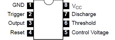
Pinout

  Connection Diagram


Specifications

Power Supply Voltage (Note 2), VDD . . . . . . . . . . . . . . . . . . . . . . . . . . . . . . . . . . . . . . . . . . . . . . . . . . 18V
Input Voltage Range (Any Input), VI . . . . . . . . . . . . . . . . . . . . . . . . . . . . . . . . . . . . . . . . . . . . 0.3 to VDD
Sink Current, Discharge or Output . . . . . . . . . . . . . . . . . . . . . . . . . . . . . . . . . . . . . . . . . . . . . . . 150mA
Source Current, Output, IO . . . . . . . . . . . . . . . . . . . . . . . . . . . . . . . . . . . . . . . . . . . . . . . . . . . . .  15mA
Continuous Total Power Dissipation, PD . . . . . . . . . . . . . . . . . . . . . . . . . . . . . . . . . . . . . . . . . 1000mW
Derate Above 25 . . . . . . . . . . . . . . . . . . . . . . . . . . . . . . . . . . . . . . . . . . . . . . . . . . . . . . . . . . 8mW/
Operating Temperature Range, TA . . . . . . . . . . . . . . . . . . . . . . . . . . . . . . . . . . . . . . . . . .. 0° to +70
Storage Temperature Range, Tstg . . . . . . . . . . . . . . . . . . . . . . . . . . . . . . . . . . . . . . . .65° to +150
Lead Temperature (During Soldering, 10sec), TL . . . . . . . . . . . . . . . . . . . . . . . . . . . . . . . . . . . . +260
Note 1. Stresses beyond those listed under "Absolute Maximum Ratings" may cause permanent damage to the device. These are stress ratings only and functional operation of the device at these or any other conditions beyond those indicated under "Recommended Operating Conditions" is not implied. Exposure to absolutemaximumrated conditions for extended periods may affect device reliability.
Note 2. All voltage values are with respect to network GND.


Description

The NTE955MC is a monolithic timing circuit in an 8Lead DIP type package fabricated using CMOS process. This timer is fully compatible with CMOS, TTL, and MOS logic and operates at frequencies up to 2MHz. Because of its high impedance, this device uses smaller timing capacitors than those used by the NE555. As a result, more accurate time delays and oscillations are possible. Power consumption is low across the full range of power supply voltage.

Like the NE555, the NTE955MC has a trigger level equal to approximately onethird of the supply voltage and a threshold level equal to approximately twothirds of the supply voltage. These levels of NTE955MC can be altered by use of the control voltage terminal (Pin5). When the trigger input (Pin2) falls below the trigger level, the flipflop is set and the output goes high. If Pin2 is above the trigger level and the threshold input (Pin6) is above the threshold level, the flipflop is reset and the output is low. The reset input (Pin4) can override all other inputs and can be used to initiate a new timing cycle. If Pin4 is low, the flipflop is reset and the output is low. Whenever the output is low, a lowimpedance path is provided between the discharge terminal (Pin7) and GND. All unused inputs of NTE955MC should be tied to an appropriate logic level to prevent false triggering.

While the CMOS output of NTE955MC  is capable of sinking over 100mA and sourcing over 10mA, the NTE955MC exhibits greatly reduced supplycurrent spikes during output transitions. This minimizes the need for the large decoupling capacitors required by the NE555.


Customers Who Bought This Item Also Bought

Margin,quality,low-cost products with low minimum orders. Secure your online payments with SeekIC Buyer Protection.
Optical Inspection Equipment
Transformers
RF and RFID
Test Equipment
Line Protection, Backups
View more