NTE943

Features: ` Wide Single Supply Volatge Range: 2.0V to 36V Dual Supplies: ±1.0V to ±18V` Low Supply Current Drain (0.8mA) Independent of Supply Voltage (1.0mW/Comparator at 5V)` Low Input Biasing Current: 25nA` Low Input Offset Current: ±5nA` Maximum Offset Voltage: ±3mV` Input CommonMode Voltage ...

product image

NTE943 Picture
SeekIC No. : 004436592 Detail

NTE943: Features: ` Wide Single Supply Volatge Range: 2.0V to 36V Dual Supplies: ±1.0V to ±18V` Low Supply Current Drain (0.8mA) Independent of Supply Voltage (1.0mW/Comparator at 5V)` Low Input Biasing Cu...

floor Price/Ceiling Price

Part Number:
NTE943
Supply Ability:
5000

Price Break

  • Qty
  • 1~5000
  • Unit Price
  • Negotiable
  • Processing time
  • 15 Days
Total Cost: $ 0.00

SeekIC Buyer Protection PLUS - newly updated for 2013!

  • Escrow Protection.
  • Guaranteed refunds.
  • Secure payments.
  • Learn more >>

Month Sales

268 Transactions

Rating

evaluate  (4.8 stars)

Upload time: 2025/1/8

Payment Methods

All payment methods are secure and covered by SeekIC Buyer Protection PLUS.

Notice: When you place an order, your payment is made to SeekIC and not to your seller. SeekIC only pays the seller after confirming you have received your order. We will also never share your payment details with your seller.
Product Details

Description


Features:

` Wide Single Supply Volatge Range: 2.0V to 36V Dual Supplies: ±1.0V to ±18V
` Low Supply Current Drain (0.8mA) Independent of Supply Voltage (1.0mW/Comparator at 5V)
` Low Input Biasing Current: 25nA
` Low Input Offset Current: ±5nA
` Maximum Offset Voltage: ±3mV
` Input CommonMode Voltage Range Includes Ground
` Differential Input Voltage Range Equal to the Power Supply Voltage
` Low Output Saturation Voltage: 240mV @ 4mA
` Output Voltge Compatible with TTL, DTL, ECL, MOS, and CMOS Logic Sytems
` Available in 3 Different Case Styles: 8Lead Metal Can: NTE943 8Lead Mini DIP: NTE943M 8Lead SOIC (Surface Mount): NTE943SM


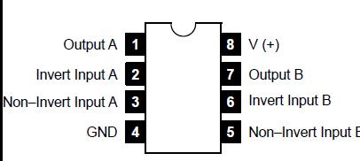
Pinout

  Connection Diagram


Specifications

Supply Voltage, V+ . . . . . . . . . . . . . . . . . . . . . . . . . . . . . . . . . . . . . . . . . . . . . . . . . . . . . . . 36V or ±18V
Differential Input Voltage (Note 1) . . . . . . . . . . . . . . . . . . . . . . . . . . . . . . . . . . . . . . . . . . . . . . . . . . 36V
Input Voltage . . . . . . . . . . . . . . . . . . . . . . . . . . . . . . . . . . . . . . . . . . . . . . . . . . . . . . . . . 0.3V to +36V
Power Dissipation (Note 2)
NTE943 . . . . . . . . . . . . . . . . . . . . . . . . . . . . . . . . . . . . . . . . . . . . . . . . . . . . . . . . . . . . . . . . . . . .660mW
NTE943M . . . . . . . . . . . . . . . . . . . . . . . . . . . . . . . . . . . . . . . . . . . . . . . . . . . . . . . . . . . . . . . . . . .780mW
NTE943SM . . . . . . . . . . . . . . . . . . . . . . . . . . . . . . . . . . . . . . . . . . . . . . . . . . . . . . . . . . . . . . . . . .510mW
Output Short Circuit to GND (Note 3) . . . . . . . . . . . . . . . . . . . . . . . . . . . . . . . . . . . . . . . . . . Continuous
Input Current (VIN < 0.3V), Note 4) . . . . . . . . . . . . . . . . . . . . . . . . . . . . . . . . . . . . . . . . . . . . . . 50mA
Operating Temperature Range . . . . . . . . . . . . . . . . . . . . . . . . . . . . . . . . . . . . . . . . . . . . .  0° to +70
Storage Temperature Range . . . . . . . . . . . . . . . . . . . . . . . . . . . . . . . . . . . . . . . . . . . .65° to +150
Lead Temperature (During Soldering, 10 sec) . . . . . . . . . . . . . . . . . . . . . . . . . . . . . . . . . . . . . . +260
Note 1. Positive excursions of input voltage may exceed the power supply level. As long as the other voltage remains within the commonmode range, the comparator will provide a proper output state. The low input voltage state must not be less than 0.3V (or 0.3V below the the magnitude of the negative power supply, if used).
Note 2. For operating at elevated temperature, these devices must be derated based on a 125maximum junction temperature and a thermal resistance of 127/W which applies for the device soldered in a printed circuit board, operating in a still air ambient. The low bias dissipation and the "ONOFF" haracteristic of the output keeps the chip dissipation very small (PD 100mW), provided the output transistors are allowed to saturate.
Note 3. Short circuits from the output to V+ can cause excessive heating and eventual destruction. When considering short circuits to GND, the maximum output current is approximately 20mA independent of the magnitude of V+.
Note 4. This input current will only exist when the voltage at any of th input leads is driven negative. It is due to the collectorbase junction of the input PNP transistors becoming forward biased and thereby acting as input diode clamps. In addition to this diode action, there is also lateral NPN parasitic transistor action on the IC chip. This transistor action can cause the output voltages of the comparators to go to the V+ voltage level (or to GND for a large overdrive) for the time duration that an input is driven negative. This is not destructive and normal output states will reestablish when the input voltage, which was negative, again returns to a value greater than 0.3V.


Description

The NTE943, NTE943M, and NTE943SM consist of two independent precision voltage comparators with an offset voltage speciication as low as 2.0mV max for two comparators which were designed specifically to operate from a single power supply over a wid range of voltages. Operation from split power supplies is also possible and the low power supply current drain is independent of the magnitude of the power supply voltage. These comparators alos have a unique characteristic in that the input commonmode voltage range includesground, even though operated from a single powe supply voltage.

Application areas of NTE943 include limit comparators, simple analog to digital converters; pulse, squarewave and time delay generators; wide range VCO; MOS clock timers; multivibrators and high voltage digital logic gates. These NTE943 are designed to directly interface with TTL and CMOS. When operated from both plus and minus power supplies they will directly interface with MOS logic where their low power drain is a distinct advantage over standard comparators.


Customers Who Bought This Item Also Bought

Margin,quality,low-cost products with low minimum orders. Secure your online payments with SeekIC Buyer Protection.
LED Products
Cables, Wires
Fans, Thermal Management
Isolators
Line Protection, Backups
RF and RFID
View more