NL27WZ16

Features: • Extremely High Speed: tPD 2.0 ns (typical) at VCC = 5.0 V• Designed for 1.65 V to 5.5 V VCC Operation• Over Voltage Tolerant Inputs• LVTTL Compatible − Interface Capability With 5.0 V TTL Logic with VCC = 3.0 V• LVCMOS Compatible• 24 mA Balance...

product image

NL27WZ16 Picture
SeekIC No. : 004434709 Detail

NL27WZ16: Features: • Extremely High Speed: tPD 2.0 ns (typical) at VCC = 5.0 V• Designed for 1.65 V to 5.5 V VCC Operation• Over Voltage Tolerant Inputs• LVTTL Compatible − Inte...

floor Price/Ceiling Price

Part Number:
NL27WZ16
Supply Ability:
5000

Price Break

  • Qty
  • 1~5000
  • Unit Price
  • Negotiable
  • Processing time
  • 15 Days
Total Cost: $ 0.00

SeekIC Buyer Protection PLUS - newly updated for 2013!

  • Escrow Protection.
  • Guaranteed refunds.
  • Secure payments.
  • Learn more >>

Month Sales

268 Transactions

Rating

evaluate  (4.8 stars)

Upload time: 2025/1/8

Payment Methods

All payment methods are secure and covered by SeekIC Buyer Protection PLUS.

Notice: When you place an order, your payment is made to SeekIC and not to your seller. SeekIC only pays the seller after confirming you have received your order. We will also never share your payment details with your seller.
Product Details

Description


Features:

• Extremely High Speed: tPD 2.0 ns (typical) at VCC = 5.0 V
• Designed for 1.65 V to 5.5 V VCC Operation
• Over Voltage Tolerant Inputs
• LVTTL Compatible − Interface Capability With 5.0 V TTL Logic with VCC = 3.0 V
• LVCMOS Compatible
• 24 mA Balanced Output Sink and Source Capability
• Near Zero Static Supply Current Substantially Reduces System Power Requirements
• Chip Complexity: FET = 72; Equivalent Gate = 18


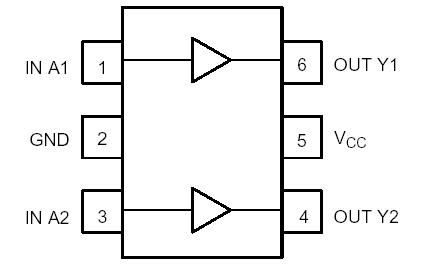
Pinout

  Connection Diagram


Specifications

Symbol Parameter Value Unit
VCC DC Supply Voltage -0.5 to +7.0 V
VI DC Input Voltage -0.5 VI +7.0 V
VO DC Output Voltage Output in Higher or Low State (Note 1) -0.5 VI +7.0 V
IIK DC Input Diode Current VI < GND −50 mA
IOK DC Output Diode Current VO = GND
VO = VCC
−50

mA
IOU DC Output Sink Current ±50 mA
ICC DC Supply Current per Supply Pin ±50 mA
IGND DC Ground Current per Ground Pin ±50 mA
TSTG Storage Temperature Range −65 to +150 °C
PD Power Dissipation in Still Air at 85°C 200 mW
JA Thermal Resistance SOT- 353 (Note 1)
SOT- 553
333 °C/W
TL Lead Temperature, 1 mm from Case for 10 Seconds 260 °C
TJ Junction Temperature Under Bias +150 °C
VESD ESD Classification Human Body Model (Note 4)
Machine Model (Note 5)
Charge Device Model (Note 6)
>2000
>200
N/A
V
ILatch−Up Latch−Up Performance Above VCC and Below GND at 85°C (Note 5) ±500 mA

1. Absolute maximum continuous ratings are those values beyond which damage to the device may occur. Exposure to these conditions or conditions beyond those indicated may adversely affect device reliability. Functional operation under absolute−maximum−rated conditions is not implied.
2. IO absolute maximum rating must be observed.
3. Tested to EIA/JESD22−A114−A
4. Tested to EIA/JESD22−A115−A
5. Tested to JESD22−C101−A
6. Tested to EIA/JESD78


Description

The NL27WZ16 is a high performance dual buffer operating from a 1.65 to 5.5 V supply. At VCC = 3 V, high impedance TTL compatible inputs significantly reduce current loading to input drivers while TTL compatible outputs offer improved switching noise performance.


Customers Who Bought This Item Also Bought

Margin,quality,low-cost products with low minimum orders. Secure your online payments with SeekIC Buyer Protection.
Industrial Controls, Meters
LED Products
Computers, Office - Components, Accessories
Hardware, Fasteners, Accessories
Resistors
Optical Inspection Equipment
View more