NL17SZ74

Features: • Extremely High Speed: tPD 2.6 ns (typical) at VCC = 5 V• Designed for 1.65 V to 5.5 V VCC Operation• 5 V Tolerant Inputs Interface Capability with 5 V TTL Logic• LVTTL Compatible• LVCMOS Compatible• 24 mA Balanced Output Sink and Source Capability&#...

product image

NL17SZ74 Picture
SeekIC No. : 004434693 Detail

NL17SZ74: Features: • Extremely High Speed: tPD 2.6 ns (typical) at VCC = 5 V• Designed for 1.65 V to 5.5 V VCC Operation• 5 V Tolerant Inputs Interface Capability with 5 V TTL Logic•...

floor Price/Ceiling Price

Part Number:
NL17SZ74
Supply Ability:
5000

Price Break

  • Qty
  • 1~5000
  • Unit Price
  • Negotiable
  • Processing time
  • 15 Days
Total Cost: $ 0.00

SeekIC Buyer Protection PLUS - newly updated for 2013!

  • Escrow Protection.
  • Guaranteed refunds.
  • Secure payments.
  • Learn more >>

Month Sales

268 Transactions

Rating

evaluate  (4.8 stars)

Upload time: 2025/1/8

Payment Methods

All payment methods are secure and covered by SeekIC Buyer Protection PLUS.

Notice: When you place an order, your payment is made to SeekIC and not to your seller. SeekIC only pays the seller after confirming you have received your order. We will also never share your payment details with your seller.
Product Details

Description


Features:

• Extremely High Speed: tPD 2.6 ns (typical) at VCC = 5 V
• Designed for 1.65 V to 5.5 V VCC Operation
• 5 V Tolerant Inputs Interface Capability with 5 V TTL Logic
• LVTTL Compatible
• LVCMOS Compatible
• 24 mA Balanced Output Sink and Source Capability
• Near Zero Static Supply Current (10 mA) Substantially Reduces System Power Requirements
• Replacement for NC7SZ74
• Tiny Ultra Small Package Only 2.1 X 3.0 mm
• High ESD Ratings: 2000 V Human Body Model High ESD Ratings: 200 V Machine Model
• Chip Complexity: FET = 64


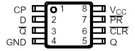
Pinout

  Connection Diagram


Specifications

Symbol Parameter Value Unit
VCC DC Supply Voltage -0.5 to +7.0 V
VI DC Input Voltage -0.5 to +7.0 V
VO DC Output Voltage Output in Higher or Low State (Note 1) −0.5 to VCC +0.5 V
IIK DC Input Diode Current VI < GND ±50 mA
IOK DC Output Diode Current VO = GND
VO = VCC
−50
+50
mA
IOU DC Output Sink Current ±50 mA
ICC DC Supply Current per Supply Pin ±50 mA
IGND DC Ground Current per Ground Pin ±50 mA
TSTG Storage Temperature Range −65 to +150 °C
TL Lead Temperature, 1 mm from Case for 10 Seconds 260 °C
TJ Junction Temperature Under Bias +150 °C
JA Thermal Resistance SOT- 353 (Note 1)
SOT- 553
250 °C/W
PD Power Dissipation in Still Air at 85°C SOT−353
SOT−553
250 mW
MSL Moisture Sensitivity Level 1  
FR Flammability Rating Oxygen Index: 28 to 34 UL 94 V−0 @ 0.125 in  
ESD ESD Classification Human Body Model (Note 4)
Machine Model (Note 5)
Charge Device Model (Note 6)
>2000
>200
N/A
V

Maximum Ratings are those values beyond which damage to the device may occur. Exposure to these conditions or conditions beyond those indicated may adversely affect device reliability. Functional operation under absolute maximumrated conditions is not implied. Functional operation should be restricted to the Recommended Operating Conditions.
1. IO absolute maximum rating must be observed.
2. Measured with minimum pad spacing on an FR4 board, using 10 mm X 1 inch, 2 ounce copper trace with no air flow.
3. Tested to EIA/JESD22A114A.
4. Tested to EIA/JESD22A115A.
5. Tested to JESD22C101A.


Description

The NL17SZ74 is a high performance, full function Edge triggered D Flip Flop, with all the features of a standard logic device such as the 74LCX74.


Customers Who Bought This Item Also Bought

Margin,quality,low-cost products with low minimum orders. Secure your online payments with SeekIC Buyer Protection.
Power Supplies - Board Mount
Sensors, Transducers
Integrated Circuits (ICs)
Memory Cards, Modules
View more