NL17SZ16

Features: ·Tiny SOT?353 and SOT?553 Packages·Source/Sink 24 mA at 3.0 Volts·Over?Voltage Tolerant Inputs and Outputs·Chip Complexity: FETs = 20·Designed for 1.65 V to 5.5 V VCC Operation·Pb-Free Packages are AvailablePinoutSpecifications Symbol Parameter Value Unit VCC DC Supply Voltag...

product image

NL17SZ16 Picture
SeekIC No. : 004434689 Detail

NL17SZ16: Features: ·Tiny SOT?353 and SOT?553 Packages·Source/Sink 24 mA at 3.0 Volts·Over?Voltage Tolerant Inputs and Outputs·Chip Complexity: FETs = 20·Designed for 1.65 V to 5.5 V VCC Operation·Pb-Free Pac...

floor Price/Ceiling Price

Part Number:
NL17SZ16
Supply Ability:
5000

Price Break

  • Qty
  • 1~5000
  • Unit Price
  • Negotiable
  • Processing time
  • 15 Days
Total Cost: $ 0.00

SeekIC Buyer Protection PLUS - newly updated for 2013!

  • Escrow Protection.
  • Guaranteed refunds.
  • Secure payments.
  • Learn more >>

Month Sales

268 Transactions

Rating

evaluate  (4.8 stars)

Upload time: 2025/1/8

Payment Methods

All payment methods are secure and covered by SeekIC Buyer Protection PLUS.

Notice: When you place an order, your payment is made to SeekIC and not to your seller. SeekIC only pays the seller after confirming you have received your order. We will also never share your payment details with your seller.
Product Details

Description


Features:

·Tiny SOT?353 and SOT?553 Packages
·Source/Sink 24 mA at 3.0 Volts
·Over?Voltage Tolerant Inputs and Outputs
·Chip Complexity: FETs = 20
·Designed for 1.65 V to 5.5 V VCC  Operation
·Pb-Free Packages are Available


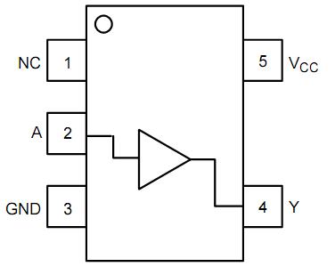
Pinout

  Connection Diagram


Specifications

Symbol Parameter Value Unit
VCC DC Supply Voltage -0.5 to +7.0 V
VI DC Input Voltage -0.5 V0 +7.0 V
VO DC Output Voltage Output in Higher or Low State (Note 1) -0.5 V0 +7.0 V
IIK DC Input Diode Current VI < GND −50 mA
IOK DC Output Diode Current VO = GND
VO = VCC
−50

mA
IOU DC Output Sink Current ±50 mA
ICC DC Supply Current per Supply Pin ±50 mA
IGND DC Ground Current per Ground Pin ±50 mA
TSTG Storage Temperature Range −65 to +150 °C
TL Lead Temperature, 1 mm from Case for 10 Seconds 260 °C
TJ Junction Temperature Under Bias +150 °C
JA Thermal Resistance SOT- 353 (Note 1)
SOT- 553
350
360
°C/W
PD Power Dissipation in Still Air at 85°C SOT−353
SOT−553
150
180
mW
MSL Moisture Sensitivity Level 1  
FR Flammability Rating Oxygen Index: 28 to 34 UL 94 V−0 @ 0.125 in  
ESD ESD Classification Human Body Model (Note 4)
Machine Model (Note 5)
Charge Device Model (Note 6)
>2000
>200
N/A
V
ILatchup Latchup PerformanceAbove VCC and Below GND at 85C (Note 6)
±500
mA

Maximum ratings are those values beyond which device damage can occur. Maximum ratings applied to the device are individual stress limit values (not normal operating conditions) and are not valid simultaneously. If these limits are exceeded, device functional operation is not implied, damage may occur and reliability may be affected.
1.Measured with minimum pad spacing on an FR4 board, using 10 mm-by-1 inch, 2?ounce copper trace with no air flow.
2.IO Absolute Maximum Rating Must be Obtained.
3.Tested to EIA/JESD22?A114-A, rated to EIA/JESD22-A114?B.
4.Tested to EIA/JESD22?A115-A, rated to EIA/JESD22-A115?A.
5.Tested to JESD22-C101-A.
6.Tested to EIA/JESD78.


Description

The NL17SZ16 is a single input Buffer in two tiny footprint packages. The device performs much as LCX multi-gate products in speed and drive.


Customers Who Bought This Item Also Bought

Margin,quality,low-cost products with low minimum orders. Secure your online payments with SeekIC Buyer Protection.
Potentiometers, Variable Resistors
Cables, Wires
Circuit Protection
Cable Assemblies
Sensors, Transducers
View more