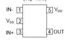
Features: ·Single Low Power SupplyVDD=1.8~5.5V·Low Offset Voltage VIO=7mV (max.)·Low Operating Current IDD=100µA(typ.)·Propagation Delay(tPLH/tPHL) 160/70ns(typ.)·Output Signal Falling Time(tTHL) 4ns(typ.)·Open Drain Output·Package Outline SC88A·C-MOS TechnologyPinoutSpecifications PARA...
NJU7119: Features: ·Single Low Power SupplyVDD=1.8~5.5V·Low Offset Voltage VIO=7mV (max.)·Low Operating Current IDD=100µA(typ.)·Propagation Delay(tPLH/tPHL) 160/70ns(typ.)·Output Signal Falling Time(tT...
SeekIC Buyer Protection PLUS - newly updated for 2013!
268 Transactions
All payment methods are secure and covered by SeekIC Buyer Protection PLUS.
PARAMETER | SYMBOL | RATING | UNIT |
Supply Voltage | VDD | 7.0 | V |
Differential Input Voltage | VID | ±7.0 (Note1) | V |
Common Mode Input Voltage | VIC | -0.3~7.0 | V |
Power Dissipation | PD | 250 (Note3) | mW |
Operating Temperature | Topr | -40 to +85 | |
Storage Temperature | Tstg | -55 to +125 |
Note1) If the supply voltage (VDD) is less than 7.0V, the input voltage must not exceed the VDD level though 7.0V is limit specified.
Note2) The output pull-up voltage must not over the VDD level.
Note3) The power dissipation is value mounted on a glass epoxy board (FR-4) in size of 50x50x1.6 millimeters square.
Note4) Decoupling capacitor should be connected between VDD and VSS due to the stabilized operation for the circuit.
The NJU7119 is super small-sized package single C-MOS comparator with open drain output.
The operating voltage of NJU7119 is from 1.8V to 5.5V. The output can drive TTL, C-MOS and various voltage levels.
The input offset voltage is lower than 7mV and the package is super small-sized SC88A. The NJU7119 is suitable for battery use items and other portable items.