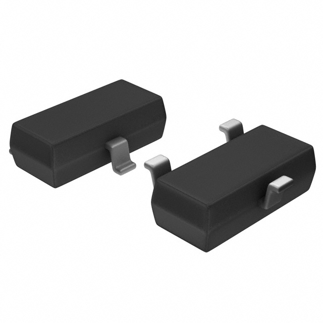
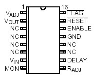
Features: • Output Voltage Options: Adjustable, 2.5 V, 3.3 V, 5.0 V• ± 2.0% Output• Low < 1.0 mA Sleep Current• Low 200 mA Quiescent Current• Fixed or Adjustable Output Voltage• Active RESET• Adjustable Reset• ENABLE• 400 mA Output Current C...
NCV8503: Features: • Output Voltage Options: Adjustable, 2.5 V, 3.3 V, 5.0 V• ± 2.0% Output• Low < 1.0 mA Sleep Current• Low 200 mA Quiescent Current• Fixed or Adjustable Out...
SeekIC Buyer Protection PLUS - newly updated for 2013!
268 Transactions
All payment methods are secure and covered by SeekIC Buyer Protection PLUS.
Rating |
Value |
Unit |
VIN (DC) |
-15 to 45 |
V |
Peak Transient Voltage (46 V Load Dump @ VIN = 14 V) |
60 |
V |
Operating Voltage |
45 |
V |
VOUT (DC) |
16 |
V |
Voltage Range (RESET, FLAG, RADJ, DELAY) |
-0.3 to 10 |
V |
Input Voltage Range: MON VADJ |
-0.3 to 10 -0.3 to 16 |
V |
Input Voltage Range (ENABLE) |
-0.3 to 10** |
V |
ESD Susceptibility (Human Body Model) (Machine Model) |
4.0 200 |
kV V |
Junction Temperature, TJ |
-40 to +150 |
|
Storage Temperature, TS |
-55 to 150 |
|
Package Thermal Resistance, SOW-16 E PAD: Junction-to-Case, RqJC Junction-to-Ambient, RqJA |
16 57 |
/W /W |
Lead Temperature Soldering: Reflow: (SMD styles only) (Note 1) |
240 peak (Note 2) |
1. 60 second maximum above 183°C.
2. −5°C/+0°C allowable conditions.
*The maximum package power dissipation must be observed.
†During the voltage range which exceeds the maximum tested voltage of VIN, operation is assured, but not specified. Wider limits may apply.
Thermal dissipation must be observed closely.
**Reference Figure 15 for switched−battery ENABLE application.
The NCV8503 is a family of precision micropower voltage regulators. Their output current capability is 400 mA.
The NCV8503 family has output voltage options for Adjustable, 2.5 V, 3.3 V and 5.0 V.
The output voltage of NCV8503 is accurate within ± 2.0% with a maximum dropout voltage of 0.6 V at 400 mA. Low quiescent current is a feature drawing less than 1.0 mA with ENABLE = 0 V. With ENABLE = 5.0 V, the part only draws 200 mA with 100 mA load. This part is ideal for any and all battery operated microprocessor equipment. Microprocessor control logic includes an active RESET (with DELAY).
The active RESET circuit operates correctly at an output voltage as low as 1.0 V. The RESET function is activated during the power up sequence or during normal operation if the output voltage drops below the regulation limits.
The reset threshold voltage can be decreased by the connection of external resistor divider to RADJ lead.The general use comparator (FLAG/Monitor) is referenced to a temperature stable voltage and provides 1.0 mA of drive current at its open collector output. The NCV8503 regulator is protected against reverse battery, short circuit, and thermal overload conditions. The device can withstand load dump transients making it suitable for use in automotive environments.
The NCV8503 has also been optimized for EMC conditions.