NCV7361A

Features: • Operating Voltage VSUP = 5.5 to 18 V• Very Low Standby Current Consumption < 110 A in Normal Mode (< 50 A in Sleep Mode)• LIN−Bus Transceiver: PNP−Bipolar Transistor Driver Slew Rate Control and Wave Shaping for Best EMC Behavior BUS Input Voltage &#...

product image

NCV7361A Picture
SeekIC No. : 004433136 Detail

NCV7361A: Features: • Operating Voltage VSUP = 5.5 to 18 V• Very Low Standby Current Consumption < 110 A in Normal Mode (< 50 A in Sleep Mode)• LIN−Bus Transceiver: PNP−Bip...

floor Price/Ceiling Price

Part Number:
NCV7361A
Supply Ability:
5000

Price Break

  • Qty
  • 1~5000
  • Unit Price
  • Negotiable
  • Processing time
  • 15 Days
Total Cost: $ 0.00

SeekIC Buyer Protection PLUS - newly updated for 2013!

  • Escrow Protection.
  • Guaranteed refunds.
  • Secure payments.
  • Learn more >>

Month Sales

268 Transactions

Rating

evaluate  (4.8 stars)

Upload time: 2025/1/8

Payment Methods

All payment methods are secure and covered by SeekIC Buyer Protection PLUS.

Notice: When you place an order, your payment is made to SeekIC and not to your seller. SeekIC only pays the seller after confirming you have received your order. We will also never share your payment details with your seller.
Product Details

Description


Features:

• Operating Voltage VSUP = 5.5 to 18 V
• Very Low Standby Current Consumption < 110 A in Normal Mode (< 50 A in Sleep Mode)
• LIN−Bus Transceiver:
PNP−Bipolar Transistor Driver
Slew Rate Control and Wave Shaping for Best EMC Behavior
BUS Input Voltage −24 V to 30 V (Independent of VSUP)
Wake−Up Via LIN Bus
Baud Rate up to 20 kBaud
Compatible to LIN Specification 1.3, 2.0 and SAE J2602
Compatible to ISO9141 Functions
• Wake−Up by LIN BUS and Startup Capable Independent of EN Voltage Level
• Linear Low Drop Voltage Regulator:
Output Voltage 5.0 V ±2%
Output Current Max. 50 mA
Output Current Limit
Overtemperature Shutdown
• Reset Time 100 ms and Reset Threshold Voltage 4.65 V
• CMOS Compatible Interface to Microcontroller
• Load Dump Protected (40 V Peak)
• Resistant Against Transient Pulses According to ISO 7637 at Pin VSUP, BUS and EN
• NCV Prefix for Automotive and Other Applications Requiring Site and Change Control


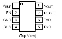
Pinout

  Connection Diagram


Specifications

Rating
Symbol
Condition
Min
Max
Unit
VSUP
VSUP
-
-1.0
30
V
T 500 ms
-
40
BUS
VBUS
-
-24
30
V
T 500 ms
-
40
Difference VSUP-VOUT
VSUP-VOUT
-
-0.3
40
V
EN
VINEN
-
-0.3
VSUP +
0.3
V
TxD, RxD, RESET
VIN
-
-0.3
VOUT +
0.3
V
EN, TxD, RxD, RESET
IIN
-
-25
25
mA
Short Circuit of Pin VSUP and VOUT
IINSH
-
-500
500
mA
ESD Capability TxD Pin
ESDBUSHB
Human Body Model, 100 pF via 1.5 k
-1.0
1.0
kV
ESD Capability on All Other Pins
ESDHB
Human Body Model, 100 pF via 1.5 k
-2.0
2.0
kV
Junction Temperature
TJ
-
-
150
Storage Temperature
TSTG
-
-55
150
Lead Temperature Soldering
Reflow: (SMD styles only)
Tsld
60 second maximum above 183°C
-5°C/+0°C allowable conditions
-
240 peak

Maximum ratings are those values beyond which device damage can occur. Maximum ratings applied to the device are individual stress limit values (not normal operating conditions) and are not valid simultaneously. If these limits are exceeded, device functional operation is not implied, damage may occur and reliability may be affected.


Description

The NCV7361A consists of a low drop voltage regulator, 5.0 V/50 mA and a LIN bus transceiver.

The NCV7361A LIN transceiver is sui table for LIN bus systems compat ible to "LIN−Protocol Specification" Rev. 1.3, 2.0 and SAE J2602.The combination of voltage regulator and bus transceiver make it ideal for a powerful and inexpensive cost effective slave node in a LIN Bus system.


Customers Who Bought This Item Also Bought

Margin,quality,low-cost products with low minimum orders. Secure your online payments with SeekIC Buyer Protection.
Prototyping Products
DE1
Computers, Office - Components, Accessories
Optoelectronics
Programmers, Development Systems
LED Products
View more