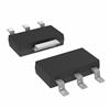
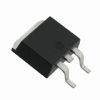
NCV494: Features: * Complete Pulse Width Modulation Control Circuitry* On-Chip Oscillator with Master or Slave Operation* On-Chip Error Amplifiers* On-Chip 5.0 V Reference* Adjustable Deadtime Control* Unco...
floor Price/Ceiling Price
- Part Number:
- NCV494
- Supply Ability:
- 5000
Price Break
- Qty
- 1~5000
- Unit Price
- Negotiable
- Processing time
- 15 Days
SeekIC Buyer Protection PLUS - newly updated for 2013!
- Escrow Protection.
- Guaranteed refunds.
- Secure payments.
- Learn more >>
Month Sales
268 Transactions
Payment Methods
All payment methods are secure and covered by SeekIC Buyer Protection PLUS.

 NCV494 Data Sheet


