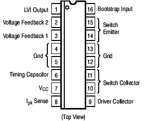
PinoutSpecifications Rating Symbol Value Unit Power Supply Voltage VCC 60 V Switch Collector Voltage Range VC(switch) -1.0 to + 60 V Switch Emitter Voltage Range VE(switch) - 2.0 to VC(switch) V Switch Collector to Emitter Voltage VCE(switch)...
NCV33163: PinoutSpecifications Rating Symbol Value Unit Power Supply Voltage VCC 60 V Switch Collector Voltage Range VC(switch) -1.0 to + 60 V Switch Emitter Voltage R...
SeekIC Buyer Protection PLUS - newly updated for 2013!
268 Transactions
All payment methods are secure and covered by SeekIC Buyer Protection PLUS.
Rating |
Symbol |
Value |
Unit |
Power Supply Voltage |
VCC |
60 |
V |
Switch Collector Voltage Range |
VC(switch) |
-1.0 to + 60 |
V |
Switch Emitter Voltage Range |
VE(switch) |
- 2.0 to VC(switch) |
V |
Switch Collector to Emitter Voltage |
VCE(switch) |
60 |
V |
Switch Current (Note 2) |
ISW |
2.5 |
A |
Driver Collector Voltage |
VC(driver) |
-1.0 to +60 |
V |
Driver Collector Current |
IC(driver) |
150 |
mA |
Bootstrap Input Current Range (Note 2) |
IBS |
-100 to +100 |
mA |
Current Sense Input Voltage Range |
VIpk (Sense) |
(VCC-7.0) to (VCC+1.0) |
V |
Feedback and Timing Capacitor Input Voltage Range |
Vin |
-1.0 to + 7.0 |
V |
Low Voltage Indicator Output Voltage Range |
VC(LVI) |
-1.0 to + 60 |
V |
Low Voltage Indicator Output Sink Current |
IC(LVI) |
10 |
mA |
Thermal Characteristics P Suffix, Dual-In-Line Case 648C Thermal Resistance, Junction-to-Air Thermal Resistance, Junction- to- Case (Pins 4, 5, 12, 13) DW Suffix, Surface Mount Case 751G Thermal Resistance, Junction-to-Air Thermal Resistance, Junction- to- Case (Pins 4, 5, 12, 13) |
RJA RJC RJA RJC |
80 15 94 18 |
/W |
Operating Junction Temperature |
TJ |
+150 |
|
Operating Ambient Temperature |
TA |
- 40 to + 115 |
|
Storage Temperature Range |
Tstg |
- 65 to +150 |
The NCV33163 series are monolithic power switching regulators that contain the primary functions required for dc-to-dc converters. This NCV33163 series is specifically designed to be incorporated in step-up, step-down, and voltage-inverting applications with a minimum number of external components. These NCV33163 devices consist of two high gain voltage feedback comparators, temperature compensated reference, controlled duty cycle oscillator, driver with bootstrap capability for increased efficiency, and a high current output switch. Protective features consist of cycle-by-cycle current limiting, and internal thermal shutdown. Also included is a low voltage indicator output designed to interface with microprocessor based systems. These NCV33163 devices are contained in a 16 pin dual-in-line heat tab plastic package for improved thermal conduction.
• Output Switch Current in Excess of 2.0 A
• Operation from 2.5 V to 60 VOC Input
• Low Standby Current
• Precision 2% Reference
• Controlled Duty Cycle Oscillator
• Driver with Bootstrap Capability for Increased Efficiency
• Cycle-by-Cycle Current Limiting
• Internal Thermal Shutdown Protection
• Low Voltage Indicator Output for Direct Microprocessor Interface
• Heat Tab Power Package
• Moisture Sensitivity Level (MSL) Equals 1
• NCV Prefix, for Automotive and Other Applications Requiring Site and Change Control