NCV33152

Features: • Pb−Free Packages are Available• Two Independent Channels with 1.5 A Totem Pole Outputs• Output Rise and Fall Times of 15 ns with 1000 pF Load• CMOS/LSTTL Compatible Inputs with Hysteresis• Undervoltage Lockout with Hysteresis• Low Standby Curre...

product image

NCV33152 Picture
SeekIC No. : 004433112 Detail

NCV33152: Features: • Pb−Free Packages are Available• Two Independent Channels with 1.5 A Totem Pole Outputs• Output Rise and Fall Times of 15 ns with 1000 pF Load• CMOS/LSTTL Co...

floor Price/Ceiling Price

Part Number:
NCV33152
Supply Ability:
5000

Price Break

  • Qty
  • 1~5000
  • Unit Price
  • Negotiable
  • Processing time
  • 15 Days
Total Cost: $ 0.00

SeekIC Buyer Protection PLUS - newly updated for 2013!

  • Escrow Protection.
  • Guaranteed refunds.
  • Secure payments.
  • Learn more >>

Month Sales

268 Transactions

Rating

evaluate  (4.8 stars)

Upload time: 2025/1/8

Payment Methods

All payment methods are secure and covered by SeekIC Buyer Protection PLUS.

Notice: When you place an order, your payment is made to SeekIC and not to your seller. SeekIC only pays the seller after confirming you have received your order. We will also never share your payment details with your seller.
Product Details

Description


Features:

• Pb−Free Packages are Available
• Two Independent Channels with 1.5 A Totem Pole Outputs
• Output Rise and Fall Times of 15 ns with 1000 pF Load
• CMOS/LSTTL Compatible Inputs with Hysteresis
• Undervoltage Lockout with Hysteresis
• Low Standby Current
• Efficient High Frequency Operation
• Enhanced System Performance with Common Switching Regulator Control ICs
• NCV Prefix for Automotive and Other Applications Requiring Site and Control Changes


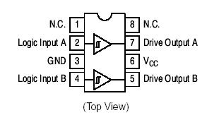
Pinout

  Connection Diagram


Specifications

Rating
Rating Symbol
Value
Unit
Power Supply Voltage
VCC
20
V
Logic Inputs (Note 1)
Vin
−0.3 to +VCC
V
Drive Outputs (Note 2)
Totem Pole Sink or Source Current
Diode Clamp Current (Drive Output to VCC)
IO
IO(clamp)
1.5
1.0
A
Power Dissipation and Thermal Characteristics
D Suffix, Plastic Package Case 751
Maximum Power Dissipation @ TA = 50°C
Thermal Resistance, Junction−to−Air
P Suffix, Plastic Package, Case 626
Maximum Power Dissipation @ TA = 50°C
Thermal Resistance, Junction−to−Air
PD
R JA
PD
R JA
0.56
180
1.0
100
W
/W
W
/W
Operating Junction Temperature
TJ
150
 
Operating Ambient Temperature MC34152
MC33152
MC33152V, NCV33152
TA
0 to +70
−40 to +85
−40 to +125
 
Storage Temperature Range
Tstg
65 to +150
Electrostatic Discharge Sensitivity (ESD)
Human Body Model (HBM)
Machine Model (MM)
ESD
2000
200
 
V
1. For optimum switching speed, the maximum input voltage should be limited to 10 V or VCC, whichever is less.
2. Maximum package power dissipation limits must be observed.


Description

The MC34152 is a dual noninverting high speed driver specifically designed to interface low current digital circuitry with power MOSFETs. MC34152 is constructed with Schottky clamped Bipolar Analog technology which offers a high degree of performance and ruggedness in hostile industrial environments.


Customers Who Bought This Item Also Bought

Margin,quality,low-cost products with low minimum orders. Secure your online payments with SeekIC Buyer Protection.
Static Control, ESD, Clean Room Products
Batteries, Chargers, Holders
Programmers, Development Systems
Cables, Wires - Management
Integrated Circuits (ICs)
View more