Features: • 0.9 V Guaranteed Operation• Standby Mode: ID = 1.9 A at 1.0 V, Typical• Rail−to−Rail Common Mode Input Voltage Range• Rail−to−Rail Output Drive Capability• No Output Phase Reversal for Over−Driven Input Signals• 0.5 mV T...
NCV2002: Features: • 0.9 V Guaranteed Operation• Standby Mode: ID = 1.9 A at 1.0 V, Typical• Rail−to−Rail Common Mode Input Voltage Range• Rail−to−Rail Output ...
SeekIC Buyer Protection PLUS - newly updated for 2013!
268 Transactions
All payment methods are secure and covered by SeekIC Buyer Protection PLUS.
US $.27 - .32 / Piece
Operational Amplifiers - Op Amps SNGL OPERATIONAL AMP 0.9V RAIL TO RAIL
US $.26 - .32 / Piece
Operational Amplifiers - Op Amps ANA SINGL OP AMP 1V 1MHZ
Rating |
Symbol |
Value |
Unit |
Supply Voltage (VCC to VEE) |
VS |
7.0 |
V |
Input Differential Voltage Range (Note 1) |
VIDR |
VEE 300 mV to 7.0 V |
V |
Input Common Mode Voltage Range (Note 1) |
VICR |
VEE 300 mV to 7.0 V |
V |
Output Short Circuit Duration (Note 2) |
tSc |
Indefinite |
sec |
Junction Temperature |
TJ |
150 |
|
Power Dissipation and Thermal Characteristics SOT23-6 Package Thermal Resistance, Junction to Air Power Dissipation @ TA = 70°C |
RJA PD |
235 340 |
/W mW |
Operating Ambient Temperature Range NCS2002 NCV2002 (Note 3) |
TA |
-40 to 105 -40 to 125 |
|
Storage Temperature Range |
Tstg |
-65 to 150 |
|
ESD Protection at any Pin Human Body Model (Note 4) |
VESD |
2000 |
V |
1. Either or both inputs should not exceed the range of VEE 300 mV to VEE + 7.0 V.
2. Maximum package power dissipation limits must be observed to ensure that the maximum junction temperature is not exceeded.
TJTA + (PD RJA)
3. NCV prefix is for automotive and other applications requiring site and change control.
4. ESD data available upon request.
The NCS2002 is an industry first sub−one volt operational amplifier that features a rail−to−rail common mode input voltage range, along with rail−to−rail output drive capability. This NCS2002 amplifier is guaranteed to be fully operational down to 0.9 V, providing an ideal solution for powering applications from a single cell Nickel Cadmium (NiCd) or Nickel Metal Hydride (NiMH) battery. Additional features include no output phase reversal with overdriven inputs, trimmed input offset voltage of 0.5 mV, extremely low input bias current of 40 pA, and a unity gain bandwidth of 1.1 MHz at 5.0 V.
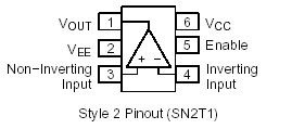
The NCS2002 also has an active high enable pin that allows external shutdown of the device. In the standby mode, the supply current is typically 1.9 A at 1.0 V. Because of its small size and enable feature, this amplifier represents the ideal solution for small portable electronic applications. The NCS2002 is available in the space saving SOT23−6 (TSOP−6) package with two industry standard pinouts.