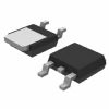
Features: • 0.2% Initial Tolerance Max.• Guaranteed Temperature Stability• Maximum 0.6 W Dynamic Impedance• Wide Operating Current Range• Directly Interchangeable with LT1009 and LM136 for Improved Performance• No Adjustments Needed for Minimum Temperature Coeff...
NCV1009: Features: • 0.2% Initial Tolerance Max.• Guaranteed Temperature Stability• Maximum 0.6 W Dynamic Impedance• Wide Operating Current Range• Directly Interchangeable with ...
SeekIC Buyer Protection PLUS - newly updated for 2013!
268 Transactions
All payment methods are secure and covered by SeekIC Buyer Protection PLUS.
• 0.2% Initial Tolerance Max.
• Guaranteed Temperature Stability
• Maximum 0.6 W Dynamic Impedance
• Wide Operating Current Range
• Directly Interchangeable with LT1009 and LM136 for Improved Performance
• No Adjustments Needed for Minimum Temperature Coefficient
• Meets Mil Std 883C ESD Requirements
• Extended Operating Temperature Range for Use in Automotive Applications
• NCV Prefix, for Automotive and Other Applications Requiring Site and Change Control
Rating |
Value |
Unit |
Reverse Current |
20 |
mA |
Forward |
10 |
mA |
Package Thermal Resistance, SO-8: Junction-to-Case, RJC Junction-to-Ambient, RJA |
45 165 |
/W /W |
Operating Temperature Range |
-40 to +125 |
|
Storage Temperature Range |
-65 to +150 |
|
Lead Temperature Soldering: Wave Solder (through hole styles only) (Note 1)Reflow: (SMD styles only) (Notes 2, 3) |
260 peak 240 peak |
Maximum ratings are those values beyond which device damage can occur. Maximum ratings applied to the device are individual stress limit values (not normal operating conditions) and are not valid simultaneously. If these limits are exceeded, device functional operation is not implied, damage may occur and reliability may be affected.
1. 10 second maximum
2. 60 second maximum above 183°C.
3. −5°C / +0°C allowable conditions.
*The maximum package power dissipation must be observed.
The NCV1009 is a precision trimmed 2.5 V ±5.0 mV shunt regulator diode.
The low dynamic impedance and wide operating current range enhances NCV1009's versatility.
The tight reference tolerance is achieved by on−chip trimming which minimizes voltage tolerance and temperature drift. A third terminal allows the reference voltage to be adjusted ±5.0% to calibrate out system errors. In many applications, the NCV1009Z can be used as a pin−to−pin replacement of the LT1009CZ and the LM136Z−2.5 with the external trim network eliminated.