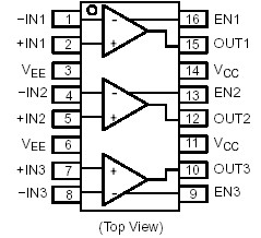
Features: • −3.0 dB Small Signal BW (AV = +2.0, VO = 0.5 Vp−p) 200 MHz Typ• Slew Rate 450 V/s• Supply Current 1.1 mA per amplifier• Input Referred Voltage Noise 4.0 nV/Hz • THD −55 dB (f = 5.0 MHz, VO = 2.0 Vp−p)• Output Current 100 mA...
NCS2530: Features: • −3.0 dB Small Signal BW (AV = +2.0, VO = 0.5 Vp−p) 200 MHz Typ• Slew Rate 450 V/s• Supply Current 1.1 mA per amplifier• Input Referred Voltage Noise 4...
SeekIC Buyer Protection PLUS - newly updated for 2013!
268 Transactions
All payment methods are secure and covered by SeekIC Buyer Protection PLUS.
US $.35 - .65 / Piece
Operational Amplifiers - Op Amps 0.9V Single Rail to Rail -40 to 105 Cel
Parameter |
Symbol |
Rating |
Unit |
Power Supply Voltage |
VS |
11 |
Vdc |
Input Voltage Range |
VI |
VS |
Vdc |
Input Differential Voltage Range |
VID |
VS |
Vdc |
Output Current |
IO |
100 |
mA |
Maximum Junction Temperature (Note 3) |
TJ |
150 |
|
Operating Ambient Temperature |
TA |
-40 to +85 |
|
Storage Temperature Range |
Tstg |
-60 to +150 |
|
Power Dissipation |
PD |
(See Graph) |
mW |
Thermal Resistance, Junctio-to-Air |
RJA |
178 |
/W |
Maximum ratings are those values beyond which device damage can occur. Maximum ratings applied to the device are individual stress limit values (not normal operating conditions) and are not valid simultaneously. If these limits are exceeded, device functional operation is not implied, damage may occur and reliability may be affected.
3. Power dissipation must be considered to ensure maximum junction temperature (TJ) is not exceeded.
NCS2530 is a triple 1.1 mA 200 MHz current feedback monolithic operational amplifier featuring high slew rate and low differential gain and phase error. The current feedback architecture allows for a superior bandwidth and low power consumption.NCS2530 features an enable pin.