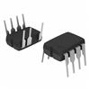
NCP1729

Features: • Operating Voltage Range of 1.15 V to 5.5 V• Output Current Capability in Excess of 50 mA• Low Current Consumption of 122A• Power Saving Shutdown Input for a Reduced Current of 0.4A• Operation at 35 kHz• Low Output Resistance of 26• Space Saving...

product image

NCP1729 Picture
SeekIC No. : 004432986 Detail

NCP1729: Features: • Operating Voltage Range of 1.15 V to 5.5 V• Output Current Capability in Excess of 50 mA• Low Current Consumption of 122A• Power Saving Shutdown Input for a Reduc...

floor Price/Ceiling Price

Part Number:
NCP1729
Supply Ability:
5000

Price Break

  • Qty
  • 1~5000
  • Unit Price
  • Negotiable
  • Processing time
  • 15 Days
Total Cost: $ 0.00

SeekIC Buyer Protection PLUS - newly updated for 2013!

  • Escrow Protection.
  • Guaranteed refunds.
  • Secure payments.
  • Learn more >>

Month Sales

268 Transactions

Rating

evaluate  (4.8 stars)

Upload time: 2025/1/9

Payment Methods

All payment methods are secure and covered by SeekIC Buyer Protection PLUS.

Notice: When you place an order, your payment is made to SeekIC and not to your seller. SeekIC only pays the seller after confirming you have received your order. We will also never share your payment details with your seller.
Product Details

Description


Features:

• Operating Voltage Range of 1.15 V to 5.5 V
• Output Current Capability in Excess of 50 mA
• Low Current Consumption of 122A
• Power Saving Shutdown Input for a Reduced Current of 0.4A
• Operation at 35 kHz
• Low Output Resistance of 26
• Space Saving TSOP−6 Package
• Pb−Free Package is Available


Application

• LCD Panel Bias
• Cellular Telephones
• Pagers
• Personal Digital Assistants
• Electronic Games
• Digital Cameras
• Camcorders
• Hand Held Instruments


Specifications

Rating

Symbol

Value

Unit

Input Voltage Range (Vin to GND)

Vin

−0.3 to 6.0

V

Output Voltage Range (Vout to GND)

Vout

−6.0 to 0.3

V

Output Current

Iout

100

mA

Output Short Circuit Duration (Vout to GND)

tSC

Indefinite

sec

Operating Junction Temperature

TJ

150

°C

Power Dissipation and Thermal Characteristics
Thermal Resistance, Junction−to−Air
Maximum Power Dissipation @ TA = 70°C

RJA
PD

256
313

°C/W

Storage Temperatur

Tstg

−55 to 150

°C

Maximum ratings are those values beyond which device damage can occur. Maximum ratings applied to the device are individual stress limit values (not normal operating conditions) and are not valid simultaneously. If these limits are exceeded, device functional operation is not implied,damage may occur and reliability may be affected.
*ESD Ratings
ESD Machine Model Protection up to 200 V, Class B
ESD Human Body Model Protection up to 2000 V, Class 2


Description

    The NCP1729 is a CMOS charge pump voltage inverter that is designed for operation over an input voltage range of 1.15 V to 5.5 V with an output current capability in excess of 50 mA. The operating current consumption is only 122 A, and a power saving shutdown input of the NCP1729 is provided to further reduce the current to a mere 0.4 A. The device contains a 35 kHz oscillator that drives four low resistance MOSFET switches, yielding a low output resistance of 26   and a voltage conversion efficiency of 99%. This device requires only two external 3.3F capacitors for a complete inverter making it an ideal solution for numerous battery powered and board level applications. The NCP1729 is available in the space saving TSOP−6 package.


Customers Who Bought This Item Also Bought

Margin,quality,low-cost products with low minimum orders. Secure your online payments with SeekIC Buyer Protection.
Optoelectronics
Soldering, Desoldering, Rework Products
Optical Inspection Equipment
Motors, Solenoids, Driver Boards/Modules
RF and RFID
Programmers, Development Systems
View more