NCP1450A

Features: • High Efficiency 86% at IO = 200 mA, VIN = 2.0 V, VOUT = 3.0 V 88% at IO = 400 mA, VIN = 3.0 V, VOUT = 5.0 V• Low Start-up Voltage of 0.9 V typical at IO = 1.0 mA• Operation Down to 0.6 V• Five Standard Voltages: 1.9 V, 2.7 V, 3.0 V, 3.3 V, 5.0 V with High Accura...

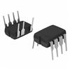
product image

NCP1450A Picture
SeekIC No. : 004432972 Detail

NCP1450A: Features: • High Efficiency 86% at IO = 200 mA, VIN = 2.0 V, VOUT = 3.0 V 88% at IO = 400 mA, VIN = 3.0 V, VOUT = 5.0 V• Low Start-up Voltage of 0.9 V typical at IO = 1.0 mA• Opera...

floor Price/Ceiling Price

Part Number:
NCP1450A
Supply Ability:
5000

Price Break

  • Qty
  • 1~5000
  • Unit Price
  • Negotiable
  • Processing time
  • 15 Days
Total Cost: $ 0.00

SeekIC Buyer Protection PLUS - newly updated for 2013!

  • Escrow Protection.
  • Guaranteed refunds.
  • Secure payments.
  • Learn more >>

Month Sales

268 Transactions

Rating

evaluate  (4.8 stars)

Upload time: 2025/1/8

Payment Methods

All payment methods are secure and covered by SeekIC Buyer Protection PLUS.

Notice: When you place an order, your payment is made to SeekIC and not to your seller. SeekIC only pays the seller after confirming you have received your order. We will also never share your payment details with your seller.
Product Details

Description


Features:

• High Efficiency 86% at IO = 200 mA, VIN = 2.0 V, VOUT = 3.0 V
                          88% at IO = 400 mA, VIN = 3.0 V, VOUT = 5.0 V
• Low Start-up Voltage of 0.9 V typical at IO = 1.0 mA
• Operation Down to 0.6 V
• Five Standard Voltages: 1.9 V, 2.7 V, 3.0 V, 3.3 V, 5.0 V with High
   Accuracy ± 2.5%
• Low Conversion Ripple
• High Output Current up to 1000 mA
   (3.0 V version at VIN = 2.0 V, L = 10 H, COUT = 220 F)
• Fixed Frequency Pulse Width Modulation (PWM) at 180 kHz
• Chip Enable Pin with On-chip 150 nA Pull-up Current Source
• Low Profile and Micro Miniature TSOP-5 Package


Application

• Personal Digital Assistant (PDA)
• Electronic Games
• Portable Audio (MP3)
• Digital Still Cameras
• Handheld Instruments


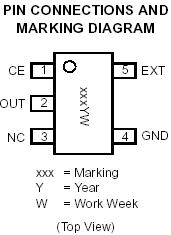
Pinout

  Connection Diagram


Specifications

Rating
Symbol
Value
Unit
Power Supply Voltage (Pin 2)
VOUT
6.0
V
Input/Output Pins
  T(Pin5)
  T Sink/Source Current


VEXT
IEXT

-0.3 to 6.0
-150 to 150

V
mA
CE(Pin1)
Input Voltage Range
Input Current Range

VCE
ICE

-0.3 to 6.0
-150 to 150

V
mA
Power Dissipation and Thermal Characteristics
Maximum Power Dissipation @ TA=25 
Thermal Resistance Junction to Air

PD
RBJA

500
250

mW
/W
Operating Ambient Temperature Range
TA
-40 to +85
Operating Junction Temprature Range
TJ
-40 to +150
Storage Temperature Range
Tstg
-55 to +150


Customers Who Bought This Item Also Bought

Margin,quality,low-cost products with low minimum orders. Secure your online payments with SeekIC Buyer Protection.
Memory Cards, Modules
Line Protection, Backups
Sensors, Transducers
RF and RFID
View more