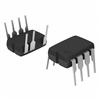
Pinout Description
The NCP1443FR4G product is 280 kHz/560 kHz switching regulators with a high efficiency, 4.0 A integrated switch.These NCP1443FR4G parts operate over a wide input voltage range,from 2.7 V to 30 V.The flexibility of the design allows the chips to operate in most power supply configurations,including boost,flyback,forward,inverting,and SEPIC.
Features of the NCP1443FR4G are:(1)pb−free packages are available;(2)integrated power switch:4.0 A guaranteed;(3)wide input range:2.7V to 30V;(4)high frequency allows for small components;(5)minimum external components;(6)easy external synchronization;(7)built−in overcurrent protection;(8)frequency foldback reduces component stress during an overcurrent condition;(9)thermal shutdown with hysteresis;(10)regulates either positive or negative output voltages;(11)shut down current:50 A maximum.Applications of the NCP1443FR4G are:(1)boost converter;(2)inverting converter;(3)distributed power;(4)portable computers;(5)battery powered systems.
The maximum ratings of the NCP1443FR4G can be summarized as:(1):the pin name is IC power input,the pin symbol is VCC,the Vmax is 30V,the Vmin is -0.3V,the Isource is N/A,the Isink is 200mA;(2):the pin name is shutdown/sync,the pin symbol is SS,the Vmax is 30V,the Vmin is -0.3V,the Isource is 1.0mA,the Isink is 1.0mA;(3):the pin name is loop compensation,the pin symbol is VC,the Vmax is 6.0V,the Vmin is -0.3V,the Isource is 10mA,the Isink is 10mA;(4):the pin name is negative feedback input (transient,10 ms),the pin symbol is NFB,the Vmax is 10V,the Vmin is -10V,the Isource is 1.0mA,the Isink is 1.0mA;(5):the pin name is test pin,the pin symbol is Test,the Vmax is 6.0V,the Vmin is -0.3V,the Isource is 1.0mA,the Isink is 1.0mA;(6):the pin name is ground,the pin symbol is GND,the Vmax is 0.3V,the Vmin is -0.3V,the Isource is 9.0mA,the Isink is 10mA;(7):the pin name is switch input,the pin symbol is VSW,the Vmax is 40V,the Vmin is -0.3V,the Isource is 10mA,the Isink is 9.0mA.

 NCP1443FR4G Data Sheet


