Features: • Extremely Low Start−Up Voltage of 0.8 V• Operation Down to Less than 0.3 V• High Efficiency 85% (Vin = 2.0 V, VOUT = 3.0 V, 70 mA)• Low Operating Current of 30 A (VOUT = 1.9 V)• Output Voltage Accuracy ± 2.5%• Low Converter Ripple with Typical ...
NCP1402: Features: • Extremely Low Start−Up Voltage of 0.8 V• Operation Down to Less than 0.3 V• High Efficiency 85% (Vin = 2.0 V, VOUT = 3.0 V, 70 mA)• Low Operating Current of...
SeekIC Buyer Protection PLUS - newly updated for 2013!
268 Transactions
All payment methods are secure and covered by SeekIC Buyer Protection PLUS.
Rating | Symbol | Value | Uni |
Power Supply Voltage (Pin2) | VOUT | 6.0 | V |
Input/Output Pins | |||
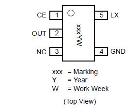
LX (Pin 5) | VLX | -0.3to 6.0 | V |
LX Peak Sink Current | ILX | 400 | mA |
CE (Pin 1) | |||
Input VOltage Range | VCE | -0.3 to 6.0 | V |
Input/Output Pins | ICE | -150 to 150 | mA |
Thermal Resistance Junction to Air | RJA | 250 | /W |
Operating Ambient Temperature Range (Note 2) | TA | -40 to + 85 | |
Operating Junction Temperature Rage | TJ | -40 to +125 | |
Storage Temperature Range | Tstg | -55 to +150 |
The NCP1402 series are monolithic power switching regulators optimized for applications where power drain must be minimized. These devices operate as variable frequency, voltage mode boost regulators and designed to operate in continuous conduction mode. Potential
applications include low powered consumer products and battery powered portable products.
The NCP1402 series are low noise variable frequency voltage−mode DC−DC converters, and consist of soft−start circuit, feedback resistor, reference voltage, oscillator, PFM comparator, PFM control circuit, current limit circuit and power switch. Due to the on−chip feedback resistor network, the system designer of NCP1402 can get the regulated output voltage from 1.8 V to 5 V with a small number of external components. The operating current is typically 30 A (VOUT = 1.9 V), and can be further reduced to about 0.6 A when the chip is disabled (VCE < 0.3 V).
The NCP1402 operation can be best understood by examining the block diagram in Figure 2. PFM comparator monitors the output voltage via the feedback resistor. When the feedback voltage is higher than the reference voltage, the power switch is turned off. As the feedback voltage is lower than reference voltage and the power switch has been off for at least a period of minimum off−time decided by PFM oscillator, the power switch is then cycled on for a period of on−time also decided by PFM oscillator, or until current limit signal is asserted. When the power switch of NCP1402 is on, current ramps up in the inductor, storing energy in the magnetic field. When the power switch is off, the energy in the magnetic field is transferred to output filter capacitor and the load. The output filter capacitor of NCP1402 stores the charge while the
inductor current is high, then holds up the output voltage until next switching cycle.