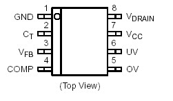
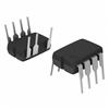
Features: • On Chip High 200 V Power Switch Circuit and Startup Circuit• Internal Startup Regulator with Auxiliary Winding Override• Operation up to 1 MHz• External Frequency Synchronization Capability• Frequency Fold−down Under Fault Conditions• Trimmed ±...
NCP1030: Features: • On Chip High 200 V Power Switch Circuit and Startup Circuit• Internal Startup Regulator with Auxiliary Winding Override• Operation up to 1 MHz• External Frequency...
SeekIC Buyer Protection PLUS - newly updated for 2013!
268 Transactions
All payment methods are secure and covered by SeekIC Buyer Protection PLUS.
Rating |
Symbol |
Value |
Unit |
Power Switch and Startup Circuits Voltage |
VDRAIN |
-0.3 to 200 |
V |
Power Switch and Startup Circuits Input Current - NCP1030 - NCP1031 |
IDRAIN |
1.0 2.0 |
A |
VCC Voltage Range |
VCC |
-0.3 to 16 |
V |
All Other Inputs/Outputs Voltage Range |
VIO |
-0.3 to 10 |
V |
VCC and All Other Inputs/Outputs Current |
IIO |
100 |
mA |
Operating Junction Temperature |
TJ |
-40 to 125 |
|
Storage Temperature |
Tstg |
-55 to 150 |
|
Power Dissipation (TJ = 25°C, 2.0 Oz., 1.0 Sq Inch Printed Circuit Copper Clad) DM Suffix, Plastic Package Case 846A D Suffix, Plastic Package Case 751 |
0.69 0.93 |
W | |
Thermal Resistance, Junction to Air (2.0 Oz. Printed Circuit Copper Clad) DM Suffix, Plastic Package Case 846A 0.36 Sq. Inch 1.0 Sq. Inch D Suffix, Plastic Package Case 751 0.36 Sq. Inch 1.0 Sq. Inch |
RJA |
181 162 135 117 |
/W |
Maximum ratings are those values beyond which device damage can occur. Maximum ratings applied to the device are individual stress limit values (not normal operating conditions) and are not valid simultaneously. If these limits are exceeded, device functional operation is not implied, damage may occur and reliability may be affected.
A. This device contains ESD protection circuitry and exceeds the following tests: Pins 1−7: Human Body Model 2000V per MIL−STD−883, Method 3015. Pins 1−7: Machine Model Method 200 V. Pin 8 is connected to the High Voltage Startup and Power Switch Circuits and rated only to the maximum voltage rating of the part, or 200 V.
B. This device contains Latchup protection and exceeds 100 mA per JEDEC Standard JESD78.
The NCP1030 and NCP1031 are a family of miniature high−voltage monolithic switching regulators with on−chip Power Switch and Startup Circuits. The NCP103x family incorporates in a single IC all the active power, control logic and protection circuitry required to implement, with minimal external components, several switching regulator applications, such as a secondary side bias supply or a low power dc−dc converter. This controller family is ideally suited for 48 V telecom, 42 V automotive and 12 V input applications. The NCP103x can be configured in any single−ended topology such as forward or flyback.
The NCP1030 is targeted for applications requiring up to 3 W, and the NCP1031 is targeted for applications requiring up to 6 W.The NCP103x internal error amplifier allows the NCP103x family to be easily configured for secondary or primary side regulation operation in isolated and non−isolated configurations.
The fixed frequency oscillator is optimized for operation up to 1 MHz and is capable of external frequency synchronization, providing additional design flexibility. In addition, the NCP103x incorporates individual line undervoltage and overvoltage detectors, cycle by cycle current limit and thermal shutdown to protect the controller under fault conditions.
The NCP103x preset current limit thresholds eliminate the need for external sensing components.