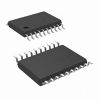
NCN6011

Features: • 2.7 to 6.0 V Input and/or Output Voltage Range• 500 nA Quiescent Supply Current• All Pins are Fully ESD Protected• Supports 10 MHz Clock• Provides a Logic I/O Enable Function• Rx/Tx Communication CapabilityApplication• SIM/GSM/SMARTCARD Interfa...

product image

NCN6011 Picture
SeekIC No. : 004432914 Detail

NCN6011: Features: • 2.7 to 6.0 V Input and/or Output Voltage Range• 500 nA Quiescent Supply Current• All Pins are Fully ESD Protected• Supports 10 MHz Clock• Provides a Logic I...

floor Price/Ceiling Price

Part Number:
NCN6011
Supply Ability:
5000

Price Break

  • Qty
  • 1~5000
  • Unit Price
  • Negotiable
  • Processing time
  • 15 Days
Total Cost: $ 0.00

SeekIC Buyer Protection PLUS - newly updated for 2013!

  • Escrow Protection.
  • Guaranteed refunds.
  • Secure payments.
  • Learn more >>

Month Sales

268 Transactions

Rating

evaluate  (4.8 stars)

Upload time: 2025/1/8

Payment Methods

All payment methods are secure and covered by SeekIC Buyer Protection PLUS.

Notice: When you place an order, your payment is made to SeekIC and not to your seller. SeekIC only pays the seller after confirming you have received your order. We will also never share your payment details with your seller.
Product Details

Description


Features:

• 2.7 to 6.0 V Input and/or Output Voltage Range
• 500 nA Quiescent Supply Current
• All Pins are Fully ESD Protected
• Supports 10 MHz Clock
• Provides a Logic I/O Enable Function
• Rx/Tx Communication Capability


Application

• SIM/GSM/SMARTCARD Interface


Pinout

  Connection Diagram  Connection Diagram


Specifications

Rating
Symbol
Value
Unit
Power Supply
VDD
7.0 V
V
External Card and Level Shifter Power Supply
SIM_VCC
7.0 V
mA
Digital Input Voltage
Digital Input Current
RESET,
IO_ENABLE
0.3 V VDD
1.0
V
mA
Digital Input Voltage
Digital Input Current
CLOCK
0.3 V VDD
1.0
V
mA
Digital Input Voltage
Digital Input Current
I/O
0.3 V VDD
1.0
V
mA
Digital Output Voltage
Digital Output Current
SIM_RST
0.3 V SIM_VCC
25
V
mA
Digital Output/Input Voltage
Digital Output/Input Current
SIM_I/O
0.3 V SIM_VCC
25
V
mA
Digital Output Voltage
Digital Output Current
SIM_CLK
0.3 V SIM_VCC
50
V
mA
Human Body Model: R = 1500 , C = 100 pF
SIM card side, pins 7, 8, 9, 10 (10, 11, 12, 13)
All other pins
ESD
4.0
2.0
kV
kV
Micro10 Package
Power Dissipation @ TA = +85°C
Thermal Resistance Junction to Air
PD
Rja
200
200
mW
°C/W
TSSOP14 Package
Power Dissipation @ TA = +85°C
Thermal Resistance Junction to Air
PD
Rja
320
125
mW
°C/W
Operating Ambient Temperature Range
TA
25 to +85
°C
Operating Junction Temperature Range
TJ
25 to +125
°C
Maximum Junction Temperature
TJmax
+150
°C
Storage Temperature Range
Tstg
65 to +150
°C
Maximum electrical ratings define the values beyond which permanent damage(s) may occur internally to the chip regardless of the operating temperature. Pin numbers in parenthesis are related to the TSSOP14 package.


Description

The NCN6011 is a level shifter analog circuit designed to translate the voltages between a SIM Card and an external microcontroller. The NCN6011 handles all the signals needed to control the data transaction between the external Card and the MPU.


Customers Who Bought This Item Also Bought

Margin,quality,low-cost products with low minimum orders. Secure your online payments with SeekIC Buyer Protection.
RF and RFID
Motors, Solenoids, Driver Boards/Modules
Undefined Category
Cables, Wires - Management
Cables, Wires
View more