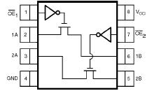
Features: Space saving US8 surface mount packageMicroPak leadless packageTypical 3 switch resistance at 5.0V VCC, VIN = 0VLevel shift facilitates 5V to 3.3V interfacingMinimal propagation delay through the switchPower down high impedance input/outputZero bounce in flow through modeTTL comp...
NC7WBD3125: Features: Space saving US8 surface mount packageMicroPak leadless packageTypical 3 switch resistance at 5.0V VCC, VIN = 0VLevel shift facilitates 5V to 3.3V interfacingMinimal propagation de...
SeekIC Buyer Protection PLUS - newly updated for 2013!
268 Transactions
All payment methods are secure and covered by SeekIC Buyer Protection PLUS.
Space saving US8 surface mount package
MicroPak leadless package
Typical 3 switch resistance at 5.0V VCC, VIN = 0V
Level shift facilitates 5V to 3.3V interfacing
Minimal propagation delay through the switch
Power down high impedance input/output
Zero bounce in flow through mode
TTL compatible active LOW control inputs
Control inputs are overvoltage tolerant
Bus switch replacement for x125 logic part
Supply Voltage (VCC) | −0.5V to +7.0V |
DC Switch Voltage (VS) | −0.5V to +7.0V |
DC Output Voltage (VIN) (Note 2) | −0.5V to +7.0V |
DC Input Diode Current(IIK) VIN < 0V | −50 mA |
DC Output (IOUT) Current | 128 mA |
DC VCC or Ground Current(ICC/IGND) | ±100 mA |
Storage Temperature Range (TSTG) | −65°C to +150°C |
Junction Temperature under Bias (TJ) |
+150°C |
Lead Temperature (TL) (Soldering, 10 Seconds) |
+260°C |
Power Dissipation (PD) @ +85°C | 250 mW |
The NC7WBD3125 is a 2-bit ultra high-speed CMOS FET bus switch with enhanced level shifting circuitry and with TTL-compatible active LOW control inputs. The low On Resistance of the switch allows inputs to be connected to outputs with minimal propagation delay and without generating additional ground bounce noise. The NC7WBD3125 is organized as a 2-bit switch with independent bus enable (OE) controls. When OE is LOW, the switch is ON and Port A is connected to Port B. When OE is HIGH, the switch is OPEN and a high-impedance state exists between the two ports. Reduced voltage drive to the gate of the FET switch permits nominal level shifting of 5V to 3V through the switch. Control inputs tolerate voltages up to 5.5V independent of VCC.