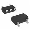
Number of Circuits
: 1
Mounting Style
: SMD/SMT
Packaging
: Reel
Supply Voltage - Max
: 5.5 V
Input Type
: Single-Ended
Maximum Operating Temperature
: + 85 C
Logic Type
: D-Type Flip-Flop
Polarity
: Inverting/Non-Inverting
Output Type
: Differential
High Level Output Current
: - 32 mA
Low Level Output Current
: 32 mA
Package / Case
: US8-8
Propagation Delay Time
: 7 ns
Logic Family
: 7S
Pinout Description
The NC7SZ74K8X is a kind of single D-type CMOS Flip-Flop. The device is fabricated with advanced CMOS technology to achieve ultra high speed with high output drive while maintaining low static power dissipation over a very broad VCC operating range. The device operates over the 1.65 V to 5.5 V VCC range. The inputs and output of NC7SZ74K8X are high impedance when VCC is 0 V. Inputs tolerate voltages up to 7 V independent of VCC operating voltage. In addition, the signal level applied to the D input is transferred to the Q output during the positive going transition of the CLK pulse.
There are some features of NC7SZ74K8X as follows: (1)space saving US8 surface mount package; (2)ultra high speed; tPD 2.6 ns typ into 50 pF at 5V VCC; (3)high output drive; ±24 mA at 3 V VCC; (4)broad VCC operating range; 1.65 V to 5.5 V; (5)power down high impedance inputs/output; (6)overvoltage tolerant inputs facilitate 5 V to 3 V translation; (7)patented noise/EMI reduction circuitry implemented.
The following is about the absolute maximum ratings of NC7SZ74K8X : (1)supply voltage (VCC): -0.5 to +7.0V; (2)DC input voltage (VIN): -0.5 to +7.0V; (3)DC output voltage (VOUT): -0.5 to +7.0V; (4)DC input diode current (IIK) when VIN < 0 V: -50 mA; (5)DC output diode current (IOK) when VOUT < 0 V: -50 mA; (6)DC output (IOUT) source/sink current: ±50 mA; (7)DC VCC/GND current (ICC/IGND): ±50 mA; (8)storage temperature range (TSTG): -65 to +150; (9)junction temperature under bias (TJ): 150; (10)junction lead temperature (TL) (Soldering, 10 seconds): 260; (11)power dissipation (PD) @ +85: 250 mW.
The last one is about the recommended operating conditions of NC7SZ74K8X: (1)power supply: operating (VCC): 1.65 to 5.5 V; data retention: 1.5 to 5.5 V; (2)input voltage (VIN): 0 to 5.5 V; (3)output voltage (VOUT): active state: 0 to VCC; 3-STATE: 0 to 5.5 V; (4)input rise and fall time (tr, tf): 0 to 20 ns/V when VCC=1.8 V, 2.5 V±0.2 V, 0 to 10 ns/V when VCC=3.3±0.3 V and 0 to 5 ns/V when VCC=5.5 V±0.5 V ; (5)operating temperature (TA): -40 to +85; (6)thermal resistance (JA): 250/W.
Parameters: | Technical/Catalog Information | NC7SZ74K8X |
| Vendor | Fairchild Semiconductor (VA) |
| Category | Integrated Circuits (ICs) |
| Mounting Type | Surface Mount |
| Package / Case | US8, 8-VSSOP |
| Function | Set and Reset |
| Number of Bits per Element | 1 |
| Number of Elements | 1 - Single |
| Current - Output High, Low | 32mA, 32mA |
| Output Type | Differential |
| Trigger Type | Positive Edge |
| Type | D-Type |
| Packaging | Digi-Reel? |
| Operating Temperature | -40°C ~ 85°C |
| Delay Time - Propagation | 6.5ns |
| Frequency - Clock | 75MHz |
| Voltage - Supply | 1.65 V ~ 5.5 V |
| Lead Free Status | Lead Free |
| RoHS Status | RoHS Compliant |
| Other Names | NC7SZ74K8X
NC7SZ74K8X
NC7SZ74K8XDKR ND
NC7SZ74K8XDKRND
NC7SZ74K8XDKR
|

 NC7SZ74K8X Data Sheet


