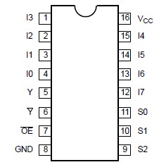
Features: • High speed 8-to-1 multiplexing• On chip decoding• Multifunction capability• Inverting and Non-Inverting outputs• Both outputs are 3-State for further multiplexer expansionPinoutSpecifications(Operation beyond the limit set forth in this table may impair th...
N74F251AD: Features: • High speed 8-to-1 multiplexing• On chip decoding• Multifunction capability• Inverting and Non-Inverting outputs• Both outputs are 3-State for further multip...
SeekIC Buyer Protection PLUS - newly updated for 2013!
268 Transactions
All payment methods are secure and covered by SeekIC Buyer Protection PLUS.
(Operation beyond the limit set forth in this table may impair the useful life of the device.
Unless otherwise noted these limits are over the operating free air temperature range.)
SYMBOL |
PARAMETER |
RATING |
UNIT |
VCC |
Supply voltage |
0.5 to +7.0 |
V |
VIN |
Input voltage |
0.5 to +7.0 |
V |
IIN |
Input current |
30 to +5 |
mA |
VOUT |
Voltage applied to output in High output state |
0.5 to VCC |
V |
IOUT |
Current applied to output in Low output state |
40 |
mA |
Tamb |
Operating free-air temperature range |
0 to +70 |
°C |
Tstg |
Storage temperature range |
65 to +150 |
°C |
The 74F251A is a logic implementation of a single 8-position switch with the switch position controlled by the state of three Select (S0, S1, S2) inputs. True (Y) and complementary (Y) outputs are both provided. The output enable (OE) is active Low. When OE is High, both outputs are in High impedance state, allowing multiple output connections to a common bus without driving nor loading the bus significantly. All but one 74F251A device must be in High impedance state to avoid high currents that would exceed the maximum ratings when the outputs of the 3-State devices are tied together. When the output of more than one 74F251A is tied together the user must ensure that there is no overlap in the active Low portion of the output enable voltages.