N74F173D

Features: • Edgetriggered Dtype register• Gated clock enable for hold do nothing mode• 3state output buffers• Gated output enable control• Speed upgrade of N8T10 and current sink upgrade• Controlled output edges to minimize ground bounces• 48mA sinking c...

product image

N74F173D Picture
SeekIC No. : 004432590 Detail

N74F173D: Features: • Edgetriggered Dtype register• Gated clock enable for hold do nothing mode• 3state output buffers• Gated output enable control• Speed upgrade of N8T10 and ...

floor Price/Ceiling Price

Part Number:
N74F173D
Supply Ability:
5000

Price Break

  • Qty
  • 1~5000
  • Unit Price
  • Negotiable
  • Processing time
  • 15 Days
Total Cost: $ 0.00

SeekIC Buyer Protection PLUS - newly updated for 2013!

  • Escrow Protection.
  • Guaranteed refunds.
  • Secure payments.
  • Learn more >>

Month Sales

268 Transactions

Rating

evaluate  (4.8 stars)

Upload time: 2025/1/9

Payment Methods

All payment methods are secure and covered by SeekIC Buyer Protection PLUS.

Notice: When you place an order, your payment is made to SeekIC and not to your seller. SeekIC only pays the seller after confirming you have received your order. We will also never share your payment details with your seller.
Product Details

Description


Features:

• Edgetriggered Dtype register
• Gated clock enable for hold "do nothing" mode
• 3state output buffers
• Gated output enable control
• Speed upgrade of N8T10 and current sink upgrade
• Controlled output edges to minimize ground bounces
• 48mA sinking capability


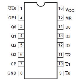
Pinout

  Connection Diagram


Specifications

SYMBOL PARAMETER
RATING
UNIT
VCC Supply voltage
0.5 to +7.0
V
VIN Input voltage
0.5 to +7.0
V
IIN Input current
30 to +5
mA
VOUT Voltage applied to output in high output state
0.5 to VCC
V
IOUT Current applied to output in low output state
96
mA
Tamb Operating free air temperature range
0 to +70
Tstg Storage temperature range
65 to +150


Description

The 74F173 is a high speed 4bit parallel load register with clock enable control, 3state buffered outputs, and master reset (MR). When the two clock enable (E0 and E1) inputs are low, the data on the D inputs is loaded into the register simultaneously with lowtohigh clock (CP) transition. When one or both enable inputs are high one setup time before the lowtohigh clock transition, the register retains the previous data.

Data inputs and clock enable inputs of 74F173 are fully edgetriggered and must be stable only one setup time before the lowtohigh clock transition.

The master reset (MR) of 74F173 is an activehigh asynchronous input. When the MR is high, all four flipflops are reset (cleared) independently of any other input condition.

The 74F173 3state output buffers are controlled by a 2input NOR gate. When both output enable (OE0 and OE1) inputs are low, the data in the register is presented at the Q output. When one or both OE inputs are high, the outputs are forced to a high impedance "off" state.

The 74F173 3state output buffers are completely independent of the register operation; the OE transition does not affect the clock and reset operations.


Customers Who Bought This Item Also Bought

Margin,quality,low-cost products with low minimum orders. Secure your online payments with SeekIC Buyer Protection.
RF and RFID
Motors, Solenoids, Driver Boards/Modules
Static Control, ESD, Clean Room Products
Crystals and Oscillators
Cables, Wires
Power Supplies - Board Mount
View more