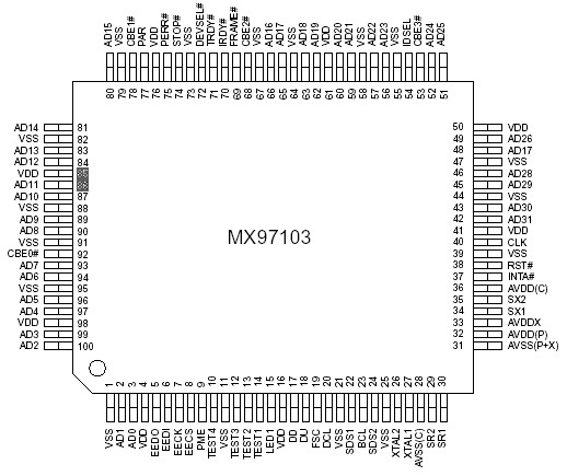
Features: • Single chip solution for ISDN PC card with PCI interface
• Supports full duplex 2B+D ISDN S/T transceiver according to ITU I.430
• Integrate S-interface, D & B channel protocol controllers, and PCI controller
• 32-bit PCI bus interface
• Each B channel has 2x64 byte FIFO for each direction
• D channel has 2x32 byte FIFO for each direction
• EEPROM interface for loading vendor-specific data
• One programmable LED
• Comply to ACPI Rev 1.0
• 0.5u CMOS
• 100-pin PQFP packagePinout Specifications
| Supply Voltage(VDD) |
4.75V to 5.25V |
| DC Input Voltage(Vin) |
-0.5V to VDD+0.5V |
| DC Output Voltage(Vout) |
-0.5V to VDD+0.5V |
| Storage Temperature Range(Tstg) |
-55 to 150 |
| Power Dissipation(PD) |
500mW |
| Lead Temp.(TL)(Soldering, 10sec) |
260 |
| ESD Rating(Rzap=1.5k, Czap=100pf) |
2000V
|
| Clamp Diode Current |
±20mA |
DescriptionMX97103 is a single chip solution for ISDN-S connection on PCI bus. It integrates S-transceiver, D and B channel protocol controllers, and PCI interface. It can be divided into the following major functional blocks : analog front end, layer 1 function, GCI interface. LAPD controller, B channel HDLC controllers, EEPROM interface and PCI interface. The important function of each major block will be described below.
According to ITU 1.430 spec. the MX97103 is a 4- wire interface. Among them, 2 wires are used for transmitting, and the other two are for receiving. The wiring configurations include short passive bus, extended passive bus and point-to-point connection. For short passive bus, the operation distance is from 100m to 200m, and the TEs(max 8)can be connected at random points along the full length of the cable. For extended passive bus, TEs connect to the cable at the far end from the NT. The total length would be at least 500m and a differential distance between TE connection points is of 25 to 50m. For point-to-point connection, the cable length can be 1km.
The analog front end deals with the signals transmitted to and received from the wiring cable. MX97103 accepts the digital data from layer 1 block and converts them into appropriate signals to be sent out to the wire, and it also receive the attenuated and distorted signal from the wire and recover them to be processed by layer 1 block. The layer 1 block comprises of PDLL, DAC, RT and MFC functions. DPLL's function is to establish S/T frame synchronization.
DAC resolves the contention issue for differnet TE accessing D channel at the same time. RT deals with the receiving S/T data extraction and put out the transmitted data at the corrent time slot. MFC is the multiframing S and Q channel control block. GCI is the digital bus for the MX97103. It can accomodate 8 GCI-compatible MX97103. This block converts the frame between GCI and S/T interface.
LAPD block relieves the microprocessor of the duty to generate HDLC frame on the D channel. It can generate flag, CRC, address and control field automatically. And it can generate S-frame for HDLC protocol. It contains 2 FIFO of 2x32 byte each to facilitate the D packet transmission and reception.
Two B channel HDLC controllers can handle tasks like flag and CRC generation, zero insertion and deletion. For each direction a 2x64 byte FIFO is provided to buffer the data.
The EEPROM interface is used to load specific vendor information after system hardware reset. Vendor ID and device ID can be load to distinguish different products.If EEPROM is not used, default values will be set.The PCI interface enables the chip attached to PCI bus directly without any glue logic. The bus speed can be from 25MHz to 33MHz.

 MX97103 Data Sheet


