MX29VW160B

Features: • Two Memory Banks for Simultaneous Read/Write operations- Host system can program or erase in one bank and simultaneously read from the other bank- Zero latency between simultaneous Read/Write operations- Read-While-Erase/Program• Extended Single-supply voltage range from 2....

product image

MX29VW160B Picture
SeekIC No. : 004431791 Detail

MX29VW160B: Features: • Two Memory Banks for Simultaneous Read/Write operations- Host system can program or erase in one bank and simultaneously read from the other bank- Zero latency between simultaneous...

floor Price/Ceiling Price

Part Number:
MX29VW160B
Supply Ability:
5000

Price Break

  • Qty
  • 1~5000
  • Unit Price
  • Negotiable
  • Processing time
  • 15 Days
Total Cost: $ 0.00

SeekIC Buyer Protection PLUS - newly updated for 2013!

  • Escrow Protection.
  • Guaranteed refunds.
  • Secure payments.
  • Learn more >>

Month Sales

268 Transactions

Rating

evaluate  (4.8 stars)

Upload time: 2024/11/26

Payment Methods

All payment methods are secure and covered by SeekIC Buyer Protection PLUS.

Notice: When you place an order, your payment is made to SeekIC and not to your seller. SeekIC only pays the seller after confirming you have received your order. We will also never share your payment details with your seller.
Product Details

Description


Features:

• Two Memory Banks for Simultaneous Read/Write operations
- Host system can program or erase in one bank and simultaneously read from the other bank
- Zero latency between simultaneous Read/Write operations
- Read-While-Erase/Program
• Extended Single-supply voltage range from 2.25V to 3.0V for read, erase and write operations
• JEDEC-standard EEPROM commands
• Minimum 100,000 write/erase cycles
• Fast Access time: 120ns
• Optimized block architecture:
- Bank A
- Eight 8K Byte (4K Word) blocks
- Three 64K Byte (32K Word) blocks
- Bank B
- Twenty-eight 64K Byte (32K Word) blocks
Data polling and toggle bit feature for detection of program or erase cycle completion
• Ready/Busy output (RY/BY): Hardware method for detection of program or erase cycle completion
• Automatic standby mode: When addresses remain stable,automatically switch themselves to low power mode(1uA Typical)
• Auto erase operation
- Automatically erases any combination of the blocks or the whole chip
- Fast erase time: 20ms typical for single block erase and 50ms typical for chip erase and multi-block erase
• Auto page program operation
- Automatically programs and verifies data at specified addresses
- Internal address and data latches for 128 Bytes (64 Word) per page in each bank
- Fast program time: 4ms typical for page program
• Built-in 128 Bytes/64 Words page buffer in each bank
- Work as SRAM for temporary data storage
- Fast access to temporary data
• Low power dissipation (typical values at 8MHz)
- 40mA typical for Read While Write
- 20mA typical for Read
- 1uA typical for standby
• Hardware reset pin (RP)
- Reset internal state machine and put the device into standby mode
• Hardware write protect pin (WP)
- Allows protection of the first two 8K Byte blocks,regardless of their orginal protect status.
• Group Protection
- Hardware method of locking groups to prevent any program or erase operation within that group
- Any group can be locked in-system or via programming equipment
- Temporary group unprotect feature allows code change in any previously locked group
• Erase Suspend/Erase Resume
- Suspends or resumes erasing blocks to allow reading and programming in other blocks.
- It is not necessary to do erase suspend if reading or programming blocks in the other bank
• Low Vcc write inhibit is equal to or less than 1.6V
• Compatible with JEDEC-standard pinouts
- 48-pin TSOP (I)
- 48-ball CSP


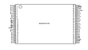
Pinout

  Connection Diagram


Specifications

RATING

VALUE

Ambient OperatingTemperature -40°C to 85°C
Storage Temperature

-65°C to 125°C

Applied Input Voltage

-0.5V to VCC + 4.5

Applied Output Voltage -0.5V to VCC + 0.6
VCC to Ground Potential -0.5V to 5.5V
A9

-0.5V to 13.0V


Description

The MX29VW160T/MX29VW160B is a 16Mbit Flash memory organized as either 2M-byte by 8-bit or 1M-word by 16-bit. To provide simultaneous operation which can read a data while program/erase,the 16Mbits of data is divided into two banks of bank A ( 2M bit) and bank B(14M bit). Bank A is organized by eight 8K-byte blocks and three 64k-byte blocks. Bank B is organized by twenty-eight 64K-byte blocks.

To allow for simple in-system operation with very low operation voltage, MX29VW160T/B can be operated with a single 2.25V to 3.0V supply voltage.Manufactured with MXIC's advanced nonvolatile memory technology, the device offers access times of 120ns, and a low 1uA typical standby current.

The MX29VW160T/MX29VW160B command set is compatible with the JEDEC single-power-supply flash standard.Commands are written to the command register using standard micro-processor write timings. MXIC's flash memory augments EPROM functionality with an internal state machine which controls the erase and program circuitry. The device RY/BY pin provides a convenient way to monitor when a program or erase cycle is complete.

Programming the MX29VW160T/MX29VW160B is performed on a page basis; 128 bytes of data are loaded into the device and then programmed simultaneously. The typical Page Program time is 4ms. The device can also be reprogrammed in standard EPROM programmers.Reading data out of the device is similar to reading from an EPROM or other flash.

Erase is accomplished by executing the Erase command sequence. This will invoke the Auto Erase algorithm which is an internal algorithm that automatically times the erase pulse widths and verifies proper cell margin.This device features both chip erase and block erase.Each block can be erased and programmed without affecting other blocks. Using MXIC's advance design technology, no preprogram is required (internally or externally). As a result, the whole MX29VW160B can be typically erased and verified in as fast as 50ms.

A combined feature of Reset Pin (RP), a hardware lockout bit, and software command sequences provide complete data protection. First, software data protection protects the device from inadvertent program or erase. Two "unlock" write cycles must be presented to the device before the program or erase command can be accepted by the device. For hardware data protection,the RP pin provide protection against unwanted command writes due to invalid system bus condition that may occur during system reset and power up/down sequence.Finally, with a hardware lockout bit feature, the MX29VW160B provides complete core security for the kernal code required for system initialization.

MXIC's flash technology reliably stores memory contents after 100,000 erase and program cycles. The MXIC's cell is designed to optimize the erase and program mechanism. In addition, the combination of advanced tunnel oxide processing and low internal electric fields for erase and program operations produce reliable cycling.

The highest degree of latch-up protection is achieved with MXIC's proprietary non-epi process. Latch-up protection is proved for stresses up to 100 milliamps on address and data pin from -1V to Vcc+1V.


Customers Who Bought This Item Also Bought

Margin,quality,low-cost products with low minimum orders. Secure your online payments with SeekIC Buyer Protection.
LED Products
Test Equipment
Inductors, Coils, Chokes
Computers, Office - Components, Accessories
View more