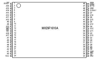
Features: • 5V ± 10% write and erase• JEDEC-standard EEPROM commands• Endurance:100,000 cycles• Fast access time: 70/90/120ns• Sector erase architecture- 16 equal sectors of 128k bytes each- Sector erase time: 1.3 s typical• Auto Erase and Auto Program Algorithm...
MX29F1610B: Features: • 5V ± 10% write and erase• JEDEC-standard EEPROM commands• Endurance:100,000 cycles• Fast access time: 70/90/120ns• Sector erase architecture- 16 equal secto...
SeekIC Buyer Protection PLUS - newly updated for 2013!
268 Transactions
All payment methods are secure and covered by SeekIC Buyer Protection PLUS.
Features: SpecificationsDescription The MX29F001T/B is a 1-mega bit Flash memory organized as 128K...
RATING |
VALUE |
Ambient Operating Temperature | 0°C to 70°C |
Storage Temperature |
-65°C to 125°C |
Applied Input Voltage |
-0.5V to VCC +7.0V |
Applied Output Voltage | -0.5V to VCC +7.0V |
VCC to Ground Potential | -0.5V to 7.0V |
A9 |
-0.5V to 13.5V |
NOTICE:
Specifications contained within the following tables are subject to change.
The MX29F1610A/MX29F1610B is a 16-mega bit Flash memory organized as either 1M wordx16 or 2M bytex8. The MX29F1610A/B includes 16-128KB(131,072) blocks or
16-64KW(65,536) blocks. MXIC's Flash memories offer the most cost-effective and reliable read/write nonvolatile random access memory. The MX29F1610A/MX29F1610B is packaged in 48-pin TSOP or 44-pin SOP. For 48-pin TSOP, CE2 and RY/BY are extra pins compared with 44- pin SOP package. This is to optimize the products (such as solid-state disk drives or flash memory cards) control pin budget. All the above three pins(CE2,RY/BY and PWD) plus one extra VCC pin are not provided in 44-pin SOP. It is designed to be reprogrammed and erased insystem or in-standard EPROM programmers.
The standard MX29F1610A/MX29F1610B offers access times as fast as 70ns,allowing operation of high-speed microprocessors without wait. To eliminate bus contention, the MX29F1610A/MX29F1610B has separate chip enables(CE1 and CE2), output enable (OE), and write enable (WE) controls.
MXIC's Flash memories augment EPROM functionality with in-circuit electrical erasure and programming. The MX29F1610A/MX29F1610B uses a command register to manage this functionality. The command register allows for 100% TTL level control inputs and fixed power supply levels during erase and programming, while maintaining maximum EPROM compatibility.
To allow for simple in-system reprogrammability, the MX29F1610A/MX29F1610B does not require high input voltages for programming. Five-volt-only commands determine the operation of the device. Reading data out of the device is similar to reading from an EPROM.
MXIC Flash technology reliably stores memory contents even after 100,000 cycles. The MXIC's cell is designed to optimize the erase and programming mechanisms. In addition, the combination of advanced tunnel oxide processing and low internal electric fields for erase and programming operations produces reliable cycling. The MX29F1610A/MX29F1610B uses a 5V ± 10% VCC supply to perform the Auto Erase and Auto Program algorithms.
The highest degree of latch-up protection is achieved with MXIC's proprietary non-epi process. Latch-up protection is proved for stresses up to 100 milliamps on address and data pin from -1V to VCC +1V.