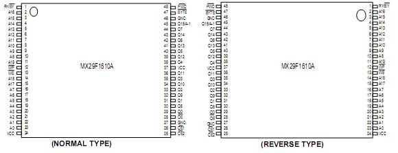
Features: * 5V ± 10% write and erase
* JEDEC-standard EEPROM commands
* Endurance:100,000 cycles
* Fast access time: 90/100/120ns
* Sector erase architecture
- 16 equal sectors of 128k bytes each
- Sector erase time: 1.3 s typical
* Auto Erase and Auto Program Algorithms
- Automatically erases any one of the sectors or the whole chip with Erase Suspend capability
- Automatically programs and verifies data at specified addresses
* Status Register feature for detection of program or erase cycle completion
* Low VCC write inhibit is equal to or less than 3.2V
* Software and hardware data protectionPinout SpecificationsRATING VALUE
Ambient Operating Temperature. 0°C to 70°C
Storage Temperature -65°C to 125°C
Applied Input Voltage -0.5V to 7.0V
Applied Output Voltage -0.5V to 7.0V
VCC to Ground Potential -0.5V to 7.0V
A9 -0.5V to 13.5VDescription The MX29F1610A is a 16-mega bit Flash memory organized as either 1M wordx16 or 2M bytex8. The MX29F1610A includes 16-128KB(131,072) blocks or 16-64KW(65,536) blocks. MXIC's Flash memories offer the most cost-effective and reliable read/write non-volatile random access memory. The MX29F1610A is packaged in 48-pin TSOP or 44-pin SOP. For 48-pin TSOP, CE2 and RY/BY are extra pins compared with 44-pin SOP package.This is to optimize the products (such as solid-state disk drives or flash memory cards) control pin budget. All the above three pins(CE2,RY/BY and PWD) plus one extra VCC pin are not provided in 44-pin SOP. It is designed to be reprogrammed and erased in-system or in-standard EPROM programmers.
The standard MX29F1610A offers access times as fast as 90ns,allowing operation of high-speed microprocessors
without wait. To eliminate bus contention, the MX29F1610A has separate chip enables(CE1 and CE2), output enable (OE), and write enable (WE) controls.
MXIC's Flash memories augment EPROM functionality with in-circuit electrical erasure and programming. The
MX29F1610A uses a command register to manage this functionality. The command register allows for 100% TTL
level control inputs and fixed power supply levels during erase and programming, while maintaining maximum
EPROM compatibility.
To allow for simple in-system reprogrammability, th MX29F1610A does not require high input voltages fo programming. Five-volt-only commands determine th operation of the device. Reading data out of the devic is similar to reading from an EPROM.
MXIC Flash technology reliably stores memory contents even after 100,000 cycles. The MXIC's cell is designed
to optimize the erase and programming mechanisms. In addition, the combination of advanced tunnel oxide
processing and low internal electric fields for erase and programming operations produces reliable cycling. The
MX29F1610A uses a 5V ! 10% VCC supply to perform the Auto Erase and Auto Program algorithms.
The highest degree of latch-up protection is achieved with MXIC's proprietary non-epi process. Latch-up protection is proved for stresses up to 100 milliamps on address and data pin from -1V to VCC +1V.

 MX29F1610A Data Sheet


