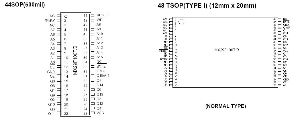
Features: • 5V 10% for read, erase and write operation• 131072x8/ 65536x16 switchable• Fast access time:55/70/90/120ns• Low power consumption - 40mA maximum active current(5MHz) - 1uA typical standby current• Command register architecture - Byte/ Word Programming (7us...
MX29F100B: Features: • 5V 10% for read, erase and write operation• 131072x8/ 65536x16 switchable• Fast access time:55/70/90/120ns• Low power consumption - 40mA maximum active current(5M...
SeekIC Buyer Protection PLUS - newly updated for 2013!
268 Transactions
All payment methods are secure and covered by SeekIC Buyer Protection PLUS.
Features: SpecificationsDescription The MX29F001T/B is a 1-mega bit Flash memory organized as 128K...
• 5V 10% for read, erase and write operation
• 131072x8/ 65536x16 switchable
• Fast access time:55/70/90/120ns
• Low power consumption
- 40mA maximum active current(5MHz)
- 1uA typical standby current
• Command register architecture
- Byte/ Word Programming (7us/ 12us typical)
- Erase (16K-Bytex1, 8K-Bytex2, 32K-Bytex1, and 64K-Byte x1)
• Auto Erase (chip) and Auto Program
- Automatically erase any combination of sectors or with Erase Suspend capability.
- Hardware method to disable any combination of sectors from program or erase operations
- Sector protect/unprotect for 5V only system or 5V/ 12V system
• 100,000 minimum erase/program cycles
• Latch-up protected to 100mA from -1 to VCC+1V
• Boot Code Sector Architecture
- T = Top Boot Sector
- B = Bottom Boot Sector
• Low VCC write inhibit is equal to or less than 3.2V
• Package type:
- 44-pin SOP
- Automatically program and verify data at specifiedaddress
• Status Reply
- Data polling & Toggle bit for detection of program and erase cycle completion.
• Compatibility with JEDEC standard
- Pinout and software compatible with single-powersupply Flash
- Superior inadvertent write protection
• Sector protection
• Ready/Busy pin(RY/BY)
- Provides a hardware method or detecting program or erase cycle completion
• Erase suspend/ Erase Resume
- Suspend an erase operation to read data from, or program data to a sector that is not being erased, then resume the erase operation.
• Hardware RESET pin
- Hardware method of resetting the device to reading the device to reading array data.
The MX29F100T/MX29F100B is a 1-mega bit Flash memory organized as 131,072 bytes or 65,536 words. MXIC's Flash memories offer the most cost-effective
and reliable read/write non-volatile random access memory. The MX29F100T/MX29F100B is packaged in 44-pin SOP and 48-pin TSOP. It is designed to be reprogrammed and erased in-system or in-standard EPROM programmers.
The standard MX29F100T/MX29F100B offers access time as fast as 55ns, allowing operation of high-speed microprocessors without wait states. To eliminate bus
contention, the MX29F100T/MX29F100B has separate chip enable (CE) and output enable (OE) controls.
MXIC's Flash memories augment EPROM functionality with in-circuit electrical erasure and programming. The MX29F100T/MX29F100B uses a command register to manage this functionality. The command register allows for 100% TTL level control inputs and organized as 131,072 bytes or 65,536 words. MXIC's Flash memories offer the most cost-effective and reliable read/write non-volatile random access fixed power supply levels during erase and programming, while maintaining maximum EPROM compatibility.