MT8LSDT3264A(I)

Features: • PC100- and PC133-compliant• JEDEC-standard 168-pin, dual in-line memory module (DIMM)• Unbuffered• 256MB (32 Meg x 64), 512MB (64 Meg x 64)• Single +3.3V ±0.3V power supply• Fully synchronous; all signals registered on positive edge of system clock&#...

product image

MT8LSDT3264A(I) Picture
SeekIC No. : 004430160 Detail

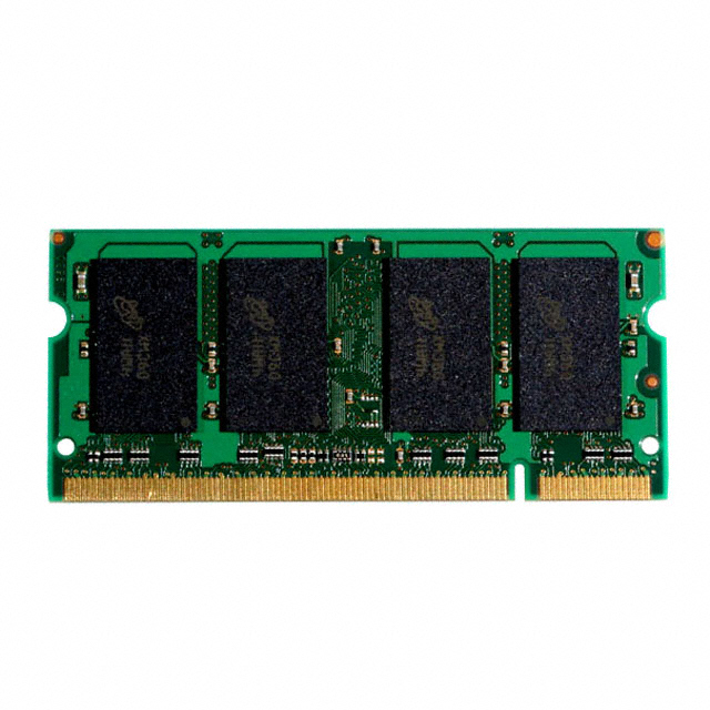
MT8LSDT3264A(I): Features: • PC100- and PC133-compliant• JEDEC-standard 168-pin, dual in-line memory module (DIMM)• Unbuffered• 256MB (32 Meg x 64), 512MB (64 Meg x 64)• Single +3.3V ±0...

floor Price/Ceiling Price

Part Number:
MT8LSDT3264A(I)
Supply Ability:
5000

Price Break

  • Qty
  • 1~5000
  • Unit Price
  • Negotiable
  • Processing time
  • 15 Days
Total Cost: $ 0.00

SeekIC Buyer Protection PLUS - newly updated for 2013!

  • Escrow Protection.
  • Guaranteed refunds.
  • Secure payments.
  • Learn more >>

Month Sales

268 Transactions

Rating

evaluate  (4.8 stars)

Upload time: 2024/8/31

Payment Methods

All payment methods are secure and covered by SeekIC Buyer Protection PLUS.

Notice: When you place an order, your payment is made to SeekIC and not to your seller. SeekIC only pays the seller after confirming you have received your order. We will also never share your payment details with your seller.
Product Details

Description


Features:

• PC100- and PC133-compliant
• JEDEC-standard 168-pin, dual in-line memory module (DIMM)
• Unbuffered
• 256MB (32 Meg x 64), 512MB (64 Meg x 64)
• Single +3.3V ±0.3V power supply
• Fully synchronous; all signals registered on positive edge of system clock
• Internal pipelined operation; column address can be changed every clock cycle
• Internal SDRAM banks for hiding row access/precharge
• Programmable burst lengths: 1, 2, 4, 8, or full page
• Auto Precharge, including Concurrent Auto Precharge, and Auto Refresh Modes
• 64ms, 8,192 cycle Auto Refresh cycle
• Self Refresh Mode
• LVTTL-compatible inputs and outputs
• Serial Presence-Detect (SPD)


Specifications

Voltage on VDD, VDDQ Supply
    Relative to VSS. . . . . . . . . . . . . . . . . . . . . -1V to +4.6V
Voltage on Inputs NC or I/O Pins
    Relative to VSS. . . . . . . . . . . . . . . . . . . . -1V to +4.6V
Operating Temperature
    TA (Commercial) . . . . . . . . . . . . . . . . .. 0°C to +70°C
    TA (Industrial). . . . . . . . . . . . . . . . . . . -40°C to +85°C
Storage Temperature (plastic) . . . . . . -55°C to +150°C
Power Dissipation, 256MB . . . . . . . . . . . . . . . . . . . . 8W
Power Dissipation, 512MB . . . . . . . . . . . . . . . . . . . 16W


Description

The MT8LSDT3264A(I) are high-speed CMOS, dynamic random-access, 256MB and 512MB memory modules organized in x64 configurations. These modules MT8LSDT3264A(I) use internally configured quad-bank SDRAMS with a synchronous interface (all signals are registered on the positive edge of the clock signals CK0-CK3).

Read and write accesses to the SDRAM modules MT8LSDT3264A(I) are burst oriented; accesses start at a selected location and continue for a programmed number of locations in a programmed sequence. Accesses begin with the registration of an ACTIVE command, which is then followed by a READ or WRITE command. The address bits of MT8LSDT3264A(I) registered coincident with the ACTIVE command are used to select the device bank and row to be accessed (BA0, BA1 select the device bank; A0A12 select the device row). The address bits registered coincident with the READ or WRITE command are used to select the starting column location for the burst access.

The modules MT8LSDT3264A(I) provide for programmable READ or WRITE burst length of 1, 2, 4, or 8 locations, or the full page, with a burst terminate option. An AUTO PRECHARGE function may be enabled to provide a selftimed row precharge that is initiateda the end of the burst sequence.

The modules MT8LSDT3264A(I) use an internal pipelined architecture to achieve high-speed operation. This architecture is compatible with the 2n rule of prefetch architectures, but it also allows the column address to be changed on every clock cycle to achieve a high-speed, fully random access. Precharging one device bank while accessing one of the other three device banks will hide the precharge cycles and provide seamless, high-speed, random- access operation.

The modules MT8LSDT3264A(I) are designed to operate in 3.3V, lowpower memory systems. An auto refresh mode is provided, along with a power-saving, power-down mode. All inputs and outputs are LVTTL-compatible.

SDRAM modules MT8LSDT3264A(I) offer substantial advances in DRAM operating performance, including the ability to syncronously burst data at a high data rate with automatic column-address generation, the ability to interleave between intenal banks in order to hide precharge time and the capability to randomly change column addresses on each clock cycle during a burst access. For more information regarding SDRAM operation, refer to the 256Mb SDRAM component data sheet.


Customers Who Bought This Item Also Bought

Margin,quality,low-cost products with low minimum orders. Secure your online payments with SeekIC Buyer Protection.
Motors, Solenoids, Driver Boards/Modules
Discrete Semiconductor Products
Line Protection, Backups
Audio Products
Potentiometers, Variable Resistors
Tapes, Adhesives
803
View more