Features: • High frequency and 100 percent bus utilization
• Fast cycle times: 6ns, 7.5ns and 10ns
• Single +3.3V ±5% power supply (VDD)
• Separate +3.3V or +2.5V isolated output buffer supply (VDDQ)
• Advanced control logic for minimum control signal interface
• Individual BYTE WRITE controls may be tied LOW
• Single R/W# (read/write) control pin
• CKE# pin to enable clock and suspend operations
• Three chip enables for simple depth expansion
• Clock-controlled and registered addresses, data I/Os and control signals
• Internally self-timed, fully coherent WRITE
• Internally self-timed, registered outputs to eliminate the need to control OE#
• SNOOZE MODE for reduced-power standby
• Common data inputs and data outputs
• Linear or Interleaved Burst Modes
• Burst feature (optional)
• Pin/function compatibility with 2Mb, 4Mb, and 18Mb ZBT SRAM
• Automatic power-down
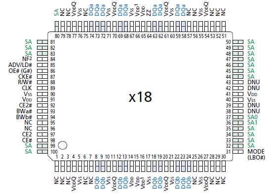
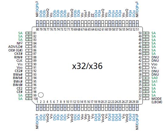
• 100-pin TQFP package
• 165-pin FBGA package
• 119-pin BGA package
Pinout
 SpecificationsVoltage on VDD Supply
Relative to VSS ................................... -0.5V to +4.6V
Voltage on VDDQ Supply
Relative to VSS ..................................... -0.5V to VDD
VIN -0.5V to VDDQ + 0.5V
Storage Temperature (plastic) .... -55°C to +150°C
Storage Temperature (FBGA) ...... -55°C to +125°C
Junction Temperature** ............................. +150°C
Short Circuit Output Current ..........................100mADescriptionThe Micron® Zero Bus Turnaround™ (ZBT®) SRAM family MT55L512L36P employs high-speed, low-power CMOS designs using an advanced CMOS process.
Micron's 8Mb ZBT SRAMs MT55L512L36P integrate a 512K x 18, 256K x 32, or 256K x 36 SRAM core with advanced synchronous peripheral circuitry and a 2-bit burst counter. These SRAMs are optimized for 100 percent bus utilization, eliminating any turnaround cycles for READ to WRITE, or WRITE to READ, transitions. All synchronous inputs of MT55L512L36P pass through registers controlled by a positive-edge-triggered single clock input (CLK). The synchronous inputs include all addresses, all data inputs, chip enable (CE#), two additional chip enables for easy depth expansion (CE2, CE2#), cycle start input (ADV/LD#), synchronous clock enable (CKE#), byte write enables (BWa#, BWb#, BWc#, and BWd#), and read/write (R/W#).
Asynchronous inputs of MT55L512L36P include the output enable (OE#, which may be tied LOW for control signal minimization), clock (CLK), and snooze enable (ZZ, which may be tied LOW if unused). There is also a burst mode pin (MODE) that selects between interleaved and linear burst modes. MODE may be tied HIGH, LOW, or left unconnected if burst is unused. The data-out (Q), enabled by OE#, is registered by the rising edge of CLK. WRITE cycles of MT55L512L36P can be from one to four bytes wide as controlled by the write control inputs.
All READ, WRITE, and DESELECT cycles of MT55L512L36P are initiated by the ADV/LD# input. Subsequent burst addresses can be internally generated as controlled by the burst advance pin (ADV/LD#). Use of burst mode is optional. It is allowable to give an address for each individual READ and WRITE cycle. BURST cycles wrap around after the fourth access from a base address.
To allow for continuous, 100 percent use of the data bus, the pipelined ZBT SRAM uses a LATE LATE WRITE cycle. For example, if a WRITE cycle begins in clock cycle one, the address is present on rising edge one. BYTE WRITEs need to be asserted on the same cycle as the address. The data associated with the address is required two cycles later, or on the rising edge of clock cycle three.
Address and write control of MT55L512L36P are registered on-chip to simplify WRITE cycles. This allows self-timed WRITE cycles. Individual byte enables allow individual bytes to be written. During a BYTE WRITE cycle, BWa# controls DQa pins; BWb# controls DQb pins; BWc# controls DQc pins; and BWd# controls DQd pins. Cycle types can only be defined when an address is loaded, i.e., when ADV/LD# is LOW. Parity/ECC bits are only available on the x36 version.
Micron's 8Mb ZBT SRAMs MT55L512L36P operate from a +3.3V VDD power supply, and all inputs and outputs are LVTTLcompatible. Users can choose either a 2.5V or 3.3V I/O version. The device is ideally suited for systems requirin high bandwidth and zero bus turnaround delays.

 MT55L512L36P Data Sheet


