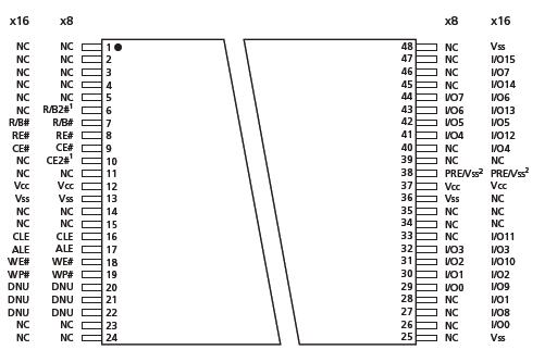
Series: -
Operating Temperature: 0°C ~ 70°C
Format - Memory: FLASH
Voltage - Supply: 2.7 V ~ 3.6 V
Interface: Parallel
Package / Case: 48-TFSOP (0.724", 18.40mm Width)
Supplier Device Package: 48-TSOP I
Memory Size: 2G (128M x 16)
Manufacturer: Micron Technology Inc
Packaging: Cut Tape (CT)
Speed: -
Memory Type: FLASH - NAND
Features: • Organization:
• Page size:
x8: 2,112 bytes (2,048 + 64 bytes)
x16: 1,056 words (1,024 + 32 words)
• Block size: 64 pages (128K + 4K bytes)
• Device size: 2Gb: 2,048 blocks; 4Gb: 4,096 blocks;
8Gb: 8,192 blocks
• Read performance:
• Random read: 25s
• Sequential read: 30ns (3V x8 only)
• Write performance:
• Page program: 300s (TYP)
• Block erase: 2ms (TYP)
• Endurance: 100,000 PROGRAM/ERASE cycles
• Data retention: 10 years
• First block (block address 00h) guaranteed to be valid without ECC (up to 1,000 PROGRAM/ERASE cycles)
• VCC: 2.7V3.6V
• Automated PROGRAM and ERASE
• Basic NAND command set:
• PAGE READ, RANDOM DATA READ, READ ID,READ STATUS, PROGRAM PAGE, RANDOM DATA INPUT, PROGRAM PAGE CACHE MODE, INTERNAL DATA MOVE, INTERNAL DATA MOVE with RANDOM DATA INPUT, BLOCK ERASE, RESET
• New commands:
• PAGE READ CACHE MODE
• READ UNIQUE ID (contact factory)
• READ ID2 (contact factory)
• Operation status byte provides a software method of detecting:
• PROGRAM/ERASE operation completion
• PROGRAM/ERASE pass/fail condition
• Write-protect status
• Ready/busy# (R/B#) pin provides a hardware method of detecting PROGRAM or ERASE cycle completion
• PRE pin: prefetch on power up
• WP# pin: hardware write protect
Pinout Specifications
|
Device |
Symbol |
MIN |
MAX |
Unit |
| MT29FxGxxxAx |
VIN |
Supply voltage on any pin relative to Vss |
-0.6 |
+4.6 |
V |
| MT29FxGxxxAx |
VCC |
| Storage temperature |
TSTG |
|
-65 |
+150 |
°C |
| Short circuit output current, I/Os |
|
|
|
5 |
mA |
Stresses greater than those listed under "Absolute Maximum Ratings" may cause permanent damage to the device. This is a stress rating only, and functional operation of the device at these or any other conditions above those indicated in the operational sections of this specification is not guaranteed. Exposure to absolute maximum rating conditions for extended periods may affect reliability.
DescriptionNAND technology of MT29F2G16AABWP provides a cost-effective solution for applications requiring highdensity solid-state storage. The MT29F2G16AABWP are 2Gb NAND Flash memory devices. The MT29F4G08BxB and MT29F4G16BxB are two-die stacks that operate as a single 4Gb device. The MT29F8G08FAB is a four-die stack that operates as two independent 4Gb devices (MT29F4G08BxB), providing a total storage capacity of 8Gb in a single, space-saving package. Micron NAND Flash devices include standard NAND features as well as new features designed to enhance system-level performance.
Micron NAND Flash devices MT29F2G16AABWP use a highly multiplexed 8- or 16-bit bus (I/O[7:0] or I/O[15:0]) to transfer data, addresses, and instructions. The five command pins (CLE,ALE, CE#, RE#, WE#) implement the NAND command bus interface protocol. Threeadditional pins control hardware write protection (WP#), monitor device status (R/B#), and initiate the auto-read feature (PRE-3V device only). Note that the PRE function is not supported on extended-temperature devices.
This hardware interface of MT29F2G16AABWP creates a low-pin-count device with a standard pinout that is the same from one density to another, allowing future upgrades to higher densities without board redesign.
MT29F2G16AABWP devices contain 2,048 and 4,096 erasable blocks respectively.Each block is subdivided into 64 programmable pages. Each page consists of 2,112 bytes (x8) or 1,056 words (x16). The pages are further divided into a 2,048-byte data storage region with a separate 64-byte area on the x8 device; and on the x16 device, separate 1,024-word and 32-word areas. The 64-byte and 32-word areas of MT29F2G16AABWP are typically used for error management functions.
The contents of each 2,112-byte page of MT29F2G16AABWP can be programmed in 300s, and an entire 132Kbyte/66K word block can be erased in 2ms. On-chip control logic automates PROGRAM and ERASE operations to maximize cycle endurance. ERASE/PROGRAM endurance is specified at 100,000 cycles when using appropriate error correcting code (ECC) and error management.

 MT29F2G16AABWP Data Sheet


