Features: • 100 MHz SDRAM-compatible read timing• Fully synchronous; all signals registered on positive edge of system clock• Internal pipelined operation; column address can be changed every clock cycle• Internal banks for hiding row access• Programmable burst length...
MT28S4M16LC: Features: • 100 MHz SDRAM-compatible read timing• Fully synchronous; all signals registered on positive edge of system clock• Internal pipelined operation; column address can be ch...
SeekIC Buyer Protection PLUS - newly updated for 2013!
268 Transactions
All payment methods are secure and covered by SeekIC Buyer Protection PLUS.
Features: • Stacked die Combo package Includes two 64Mb Flash devices Choice of either one 3...
This SyncFlash® data sheet of MT28S4M16LC is divided into two major sections. The SDRAM Interface Functional Description details compatibility with the SDRAM memory, and the Flash Memory Functional Description specifies the symmetrical-sectored flash architecture functional commands.
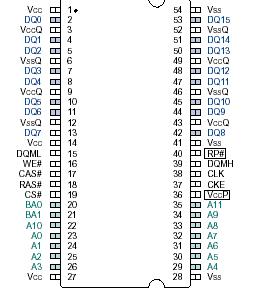
The MT28S4M16LC is a nonvolatile, electrically sector- erasable (Flash), programmable memory containing 67,108,864 bits organized as 4,194,304 words (16 bits). SyncFlash memory is ideal for 3.3V-only platforms that require both hardware and software protection modes. Additional hardware protection modes arealso available when VHH is applied to the RP# pin. Programming or erasing the device is done with a 3.3V VCCP voltage, while all other operations are performed with a 3.3V VCC. The device is fabricated with Micron's advanced CMOS floating-gate process.
The MT28S4M16LC is organized into 16 independently erasable blocks. To ensure that critical firmware is protected from accidental erasure or overwrite, the MT28S4M16LC features sixteen 256K-word hardwareand software-lockable blocks.
The MT28S4M16LC four-bank architecture supports true concurrent operations. A read access to any bank can occur simultaneously with a background PROGRAM or ERASE operation to any other bank.
The SyncFlash memory MT28S4M16LC has a synchronous interface (all signals are registered on the positive edge of the clock signal, CLK). Read accesses to the memory are burst oriented; accesses start at a selected location and continue for a programmed number of locations in a programmed sequence. Accesses begin with the registration of an ACTIVE command, followed by a READ command. The address bits registered coincident with the ACTIVE command are used to select the bank and row to be accessed. The address bits of MT28S4M16LC registered coincident with the READ command are used to select the starting column location for the burst access.
The SyncFlash memory MT28S4M16LC provides for programmable read burst lengths of 1, 2, 4, or 8 locations, or the full page, with a burst terminate option. The 4 Meg x 16 SyncFlash memory uses an internal pipelined architecture to achieve high-speed operation.
The 4 Meg x 16 SyncFlash memory MT28S4M16LC is designed to operate in 3.3V, low-power memory systems. A deep power-down mode is provided, along with a powersaving standby mode. All inputs and outputs are LVTTL-compatible.
SyncFlash memory MT28S4M16LC offers substantial advances in Flash operating performance, including the ability to synchronously burst data at a high data rate with automatic column-address generation and the capability to randomly change column addresses on each clock cycle during a burst access.